Semiconductor package structure and preparation method thereof

A packaging structure and semiconductor technology, applied in semiconductor/solid-state device manufacturing, semiconductor devices, semiconductor/solid-state device components, etc., can solve problems such as poor electrical properties and antenna performance, long transmission signal lines, and large packaging volume, etc., to achieve Good electrical and antenna performance, short transmission signal path, and low dielectric loss

Pending Publication Date: 2019-08-16
SJ SEMICON JIANGYIN CORP
View PDF0 Cites 3 Cited by
  • Summary
  • Abstract
  • Description
  • Claims
  • Application Information

AI Technical Summary

Problems solved by technology

[0003] In view of the above-mentioned shortcomings of the prior art, the object of the present invention is to provide a semiconductor packaging structure and its preparation method, which are used to solve the problems of longer transmission signal lines, lower electrical properties and antenna performance in the prior art packaging structure. Problems such as poor power consumption, large package volume, etc.

Method used


Image

  • Semiconductor package structure and preparation method thereof
  • Semiconductor package structure and preparation method thereof
  • Semiconductor package structure and preparation method thereof

Examples


Embodiment 1

[0079] see figure 1 , the invention provides a method for preparing a semiconductor package structure, the method for preparing a semiconductor package structure includes the following steps:

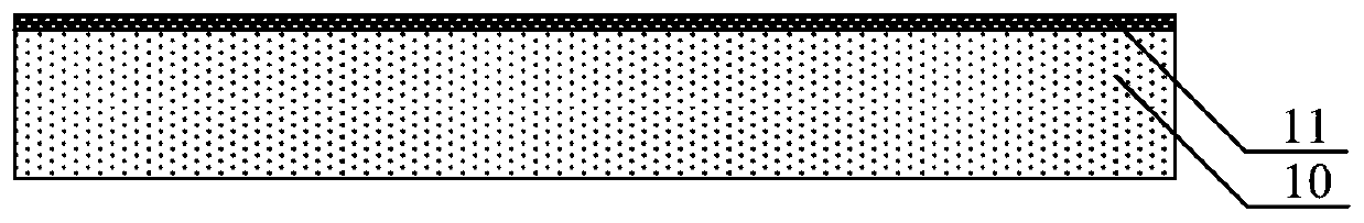
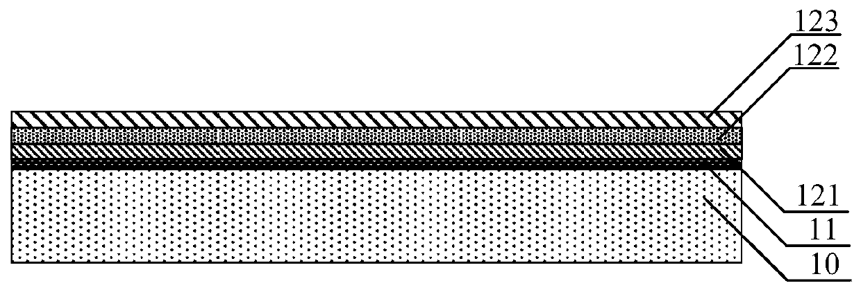
[0080] 1) providing a base, and forming a sacrificial layer on the upper surface of the base;

[0081] 2) forming a rewiring layer on the upper surface of the sacrificial layer;

[0082] 3) forming an electrical connection structure on the upper surface of the rewiring layer, the electrical connection structure being electrically connected to the rewiring layer;

[0083] 4) forming a plastic seal layer on the upper surface of the rewiring layer, and the plastic seal layer seals the electrical connection structure;

[0084] 5) forming a first antenna layer on the upper surface of the plastic sealing layer, and the first antenna layer is electrically connected to the electrical connection structure;

[0085] 6) forming a frame structure on the upper surface of the plastic sealing layer...

Embodiment 2

[0146] Please combine Figure 2 to Figure 14 Continuing to refer to 15, the present invention also provides a semiconductor package structure, the semiconductor package structure comprising: a rewiring layer 12; a chip 21, the chip 21 is flip-chip bonded to the lower surface of the rewiring layer 12, and the The chip 21 is electrically connected to the rewiring layer 12; an electrical connection structure 13, the electrical connection structure 13 is located on the upper surface of the rewiring layer 12, and the electrical connection structure 13 is electrically connected to the rewiring layer 12 Connection; the plastic sealing layer 14, the plastic sealing layer 14 is located on the upper surface of the rewiring layer 12, and the plastic sealing layer 14 plastic seals the electrical connection structure 13; the first antenna layer 15, the first antenna layer 15 Located on the upper surface of the plastic sealing layer 14, and the first antenna layer 15 is connected to the ele...


PUM


Abstract

The invention provides a semiconductor package structure and a preparation method thereof. The semiconductor package structure comprises a redistribution layer; a flip-chip bonded to the lower surfaceof the redistribution layer; an electrical connection structure on the upper surface of the redistribution layer; a plastic package layer located on the upper surface of the redistribution layer andplastically packaging the electrical connection structure; a first antenna layer located on the upper surface of the plastic package layer; a frame structure located on the upper surface of the plastic package layer and located at the periphery of the first antenna layer; a cover plate on the top of the frame structure; a second antenna layer located on the lower surface of the cover plate; solderball bumps on the lower surface of the redistribution layer. The semiconductor package structure of the invention is reduced in volume, improves the integration degree of a device, has a short transmission signal path, and can obtain good electrical properties and antenna performance.

Description

technical field [0001] The invention relates to the technical field of semiconductor packaging, in particular to a semiconductor packaging structure and a preparation method thereof. Background technique [0002] In the existing antenna mobile phone terminal applications, the antenna transmits and receives signals through the combination of multiple functional modules (such as active components and passive components) and the antenna. The traditional packaging structure is to combine each functional module And the antenna is assembled on the PCB board. In the above structure, the functional modules and antennas are arranged on the surface of the PCB board, which will occupy a large area of ​​the PCB board, so that the entire packaging structure has long lines for transmitting signals, poor electrical properties and antenna performance, and high power consumption. And the problem of large package volume. Contents of the invention [0003] In view of the above-mentioned sh...

Claims


Application Information

Patent Timeline
Patent Type & Authority Applications(China)
IPC IPC(8): H01L23/66H01L23/538H01L21/764H01L21/768H01Q1/22
CPCH01L21/764H01L21/76895H01L23/5386H01L23/66H01Q1/2283
Inventor 陈彦亨林正忠
Owner SJ SEMICON JIANGYIN CORP
Why Eureka
Try Eureka