Fabrication method of display substrate and display substrate

A technology for display substrates and display panels, which is used in the manufacture of semiconductor/solid-state devices, electrical components, and electrical solid-state devices, etc., can solve the problems of poor bottom flatness, difficult depth control, and difficulty in removing the backing film in the area where the back film is removed. The effect of ensuring the tearing yield, avoiding electrostatic discharge, and ensuring the production yield

Active Publication Date: 2019-08-27
BOE TECH GRP CO LTD +1
View PDF3 Cites 6 Cited by
  • Summary
  • Abstract
  • Description
  • Claims
  • Application Information

AI Technical Summary

Problems solved by technology

However, due to the mutual thermal influence between the laser spots, the depth of laser removal of the backing film is not easy to control, and is often accompanied by sintering residues of the backing film and pressure sensitive adhesive (PSA), and the bottom flatness of the backing film removal area is poor. And there is a risk of foreign matter, and the hot working area of ​​laser sintering is relatively large, and the sintering edge often has gaps caused by thermal deformation of the material, which affects the shape of the sintering edge and then affects the stress distribution
[0003] To sum up, it is difficult to remove the back film in the existing technology, and the process of removing the back film is prone to sintering residues, and there will also be gaps at the sintering edge, which affects the yield of the back film removal and the quality of the display product.

Method used


Image

  • Fabrication method of display substrate and display substrate
  • Fabrication method of display substrate and display substrate
  • Fabrication method of display substrate and display substrate

Examples


Embodiment Construction

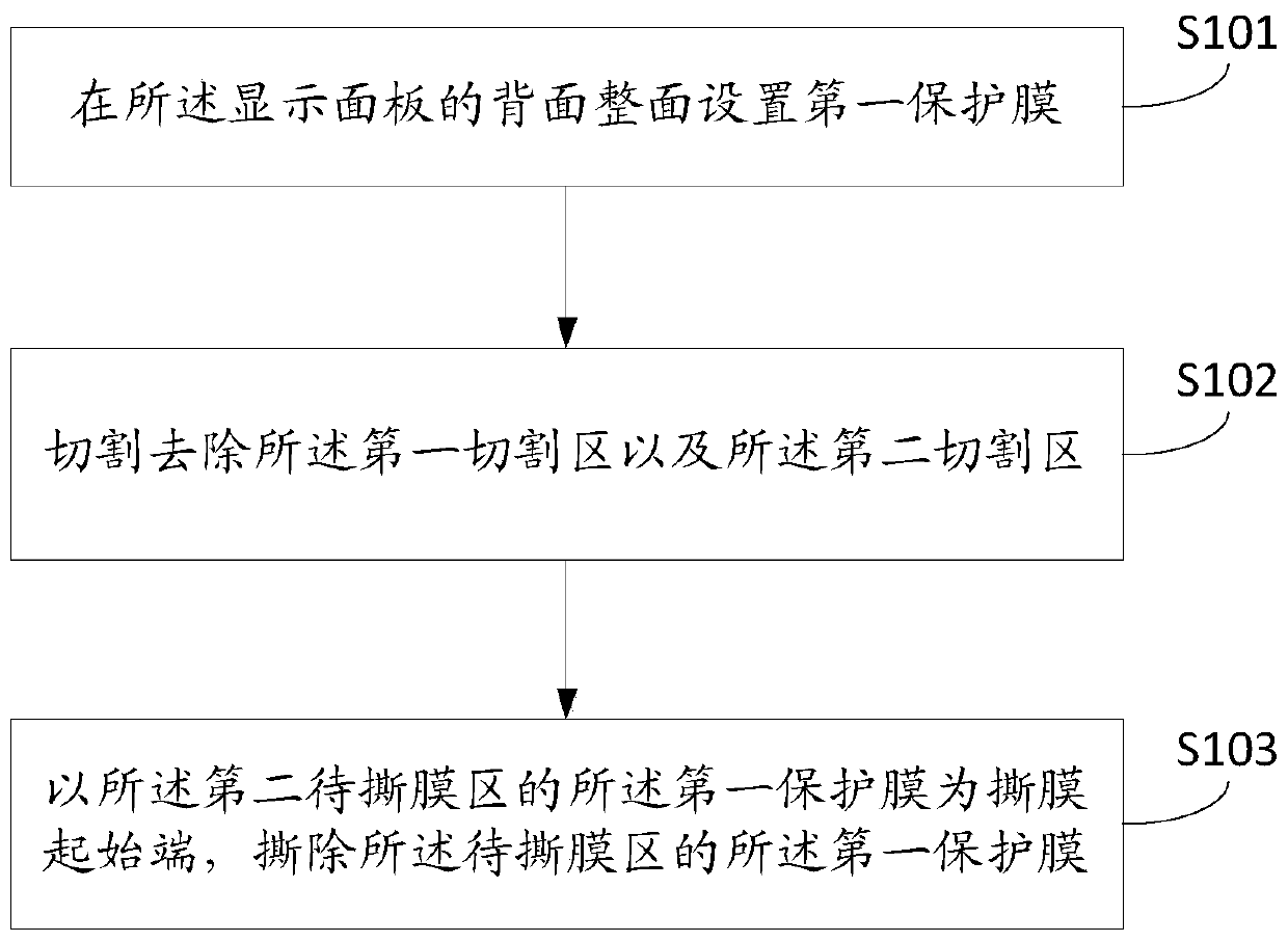
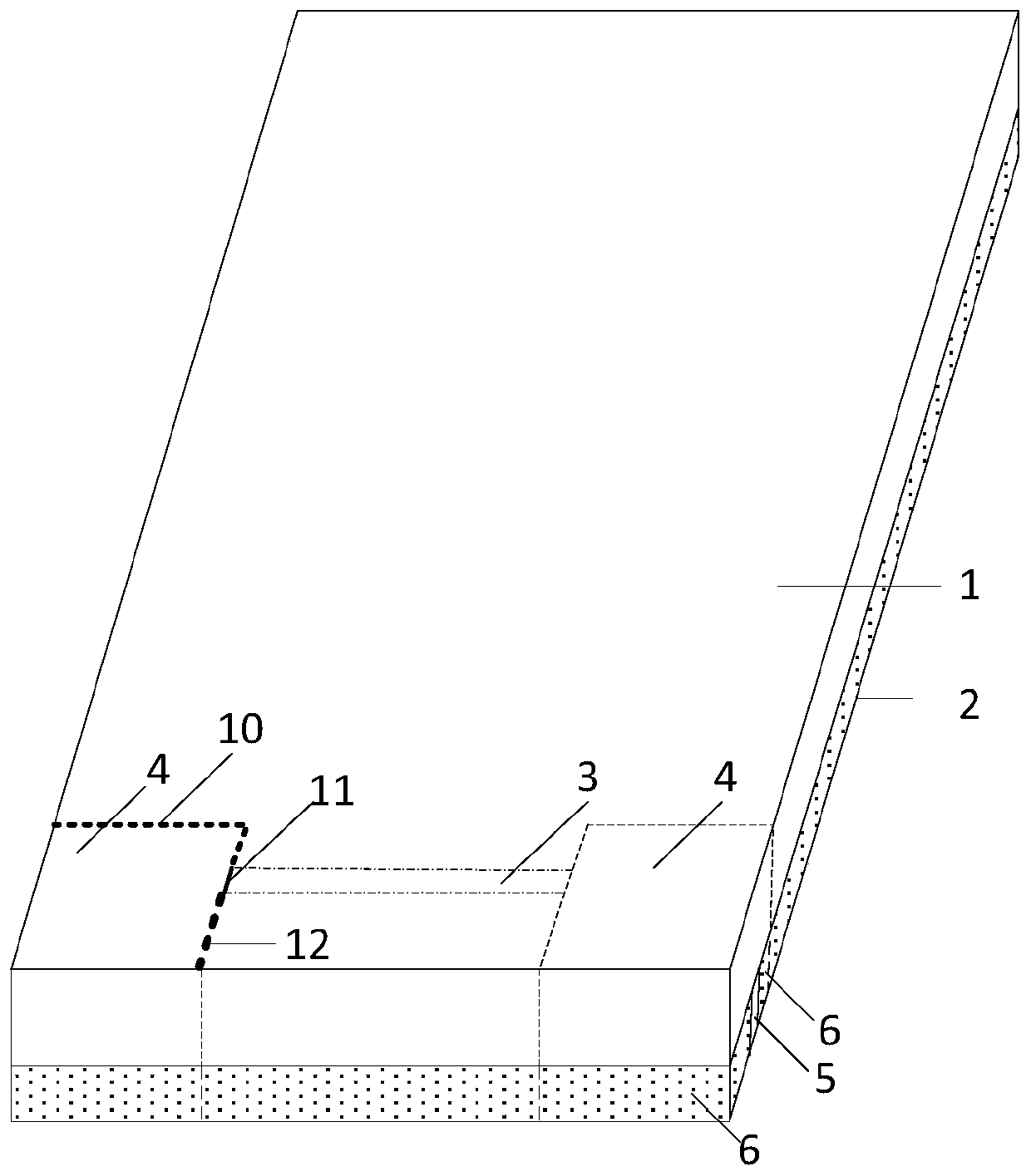
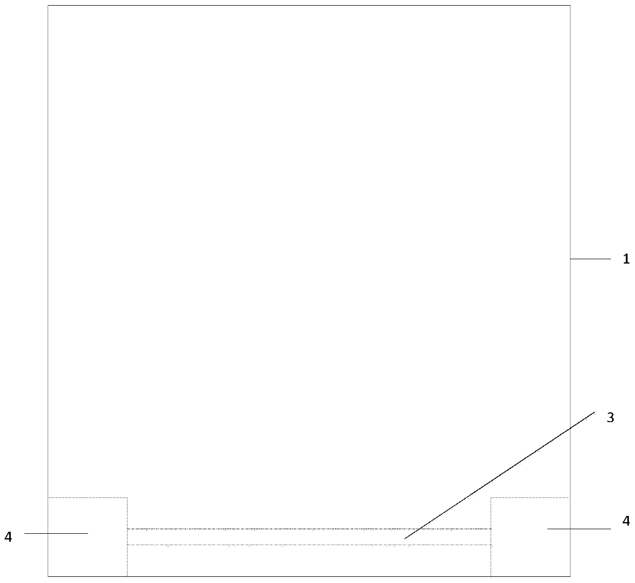
[0051] The embodiment of the present application provides a method for preparing a display substrate, such as figure 1 As shown, the method includes:

[0052] S101. Install a first protective film on the entire back surface of the display panel; wherein, the display panel has: a region to be bent, connected to the region to be bent in the extending direction of at least one region to be bent The first cutting area; the first protective film has a second cutting area and a film area to be torn, and the film area to be torn is disconnected from other areas outside the film area to be torn; the film area to be torn includes: A film area to be torn and a second film area to be torn, the first film area to be torn coincides with the area to be bent, the area formed by the second film area to be torn and the second cutting area is identical to the area formed by the second cutting area The first cutting area overlaps;

[0053] S102, cutting and removing the first cutting area and ...


PUM


Abstract

The invention discloses a fabrication method of a display substrate and the display substrate, which are used for reducing film stripping difficulty and improving film stripping yield. The fabricationmethod of the display substrate, provided by the embodiment of the invention comprises the steps of arranging a first protection film on the whole back surface of a display panel, wherein the displaypanel is provided with a to-be-bent region and a first cutting region, the first cutting region is connected with the to-be-bent region in an extension direction of at least one to-be-bent region, the first protection film is provided with a second cutting region and a to-be-torn film region, the to-be-torn film region is disconnected with other regions outside the to-be-torn film region, the to-be-torn film region comprises a first to-be-torn film region and a second to-be-torn film region, the first to-be-torn film region is coincided with the to-be-bent region, and a region comprising thesecond to-be-torn film region and the second cutting region is coincided with the first cutting region; cutting to remove the first cutting region and the second cutting region; and tearing the firstprotection film at the to-be-torn film region by taking the first protection film at the second to-be-torn film region as a film stripping initial end.

Description

technical field [0001] The present application relates to the field of display technology, in particular to a method for preparing a display substrate and the display substrate. Background technique [0002] At present, the production of full-screen Organic Light-Emitting Diode (OLED) display products requires a terminal bending process after obtaining an OLED panel with a back film attached. The terminal bending process needs to remove the back film. In the prior art, the method of removing the backing film is to use laser point input to "ablate" the grooves in the target area through a large number of dense vertical laser dot arrays, so as to remove the backing film in the bending area. However, due to the mutual thermal influence between the laser spots, the depth of the laser removal of the backing film is not easy to control, and is often accompanied by sintering residues of the backing film and pressure sensitive adhesive (PSA), and the bottom flatness of the backing ...

Claims


Application Information

Patent Timeline
Patent Type & Authority Applications(China)
IPC IPC(8): H01L51/56H01L21/683
CPCH01L21/6836H01L2221/68386H01L2221/68354H10K71/00
Inventor 赵潇龚增超赵俊杰金明焕赖鹏黄修雄王家林
Owner BOE TECH GRP CO LTD
Why Eureka
Try Eureka