Wafer grinding assembly and grinding equipment

A component and wafer technology, applied in grinding/polishing equipment, grinding devices, grinding machine tools, etc., to solve problems such as wafer surface influence and wafer surface defects

Inactive Publication Date: 2019-08-30
XIAN ESWIN SILICON WAFER TECH CO LTD
View PDF10 Cites 1 Cited by
  • Summary
  • Abstract
  • Description
  • Claims
  • Application Information

AI Technical Summary

Problems solved by technology

[0004] Embodiments of the present invention provide a wafer grinding assembly and grinding equipment to solve the problem that t

Method used


Image

  • Wafer grinding assembly and grinding equipment
  • Wafer grinding assembly and grinding equipment
  • Wafer grinding assembly and grinding equipment

Examples


Embodiment Construction

[0026] The following will clearly and completely describe the technical solutions in the embodiments of the present invention with reference to the accompanying drawings in the embodiments of the present invention. Obviously, the described embodiments are some of the embodiments of the present invention, but not all of them. Based on the embodiments of the present invention, all other embodiments obtained by persons of ordinary skill in the art without creative efforts fall within the protection scope of the present invention.

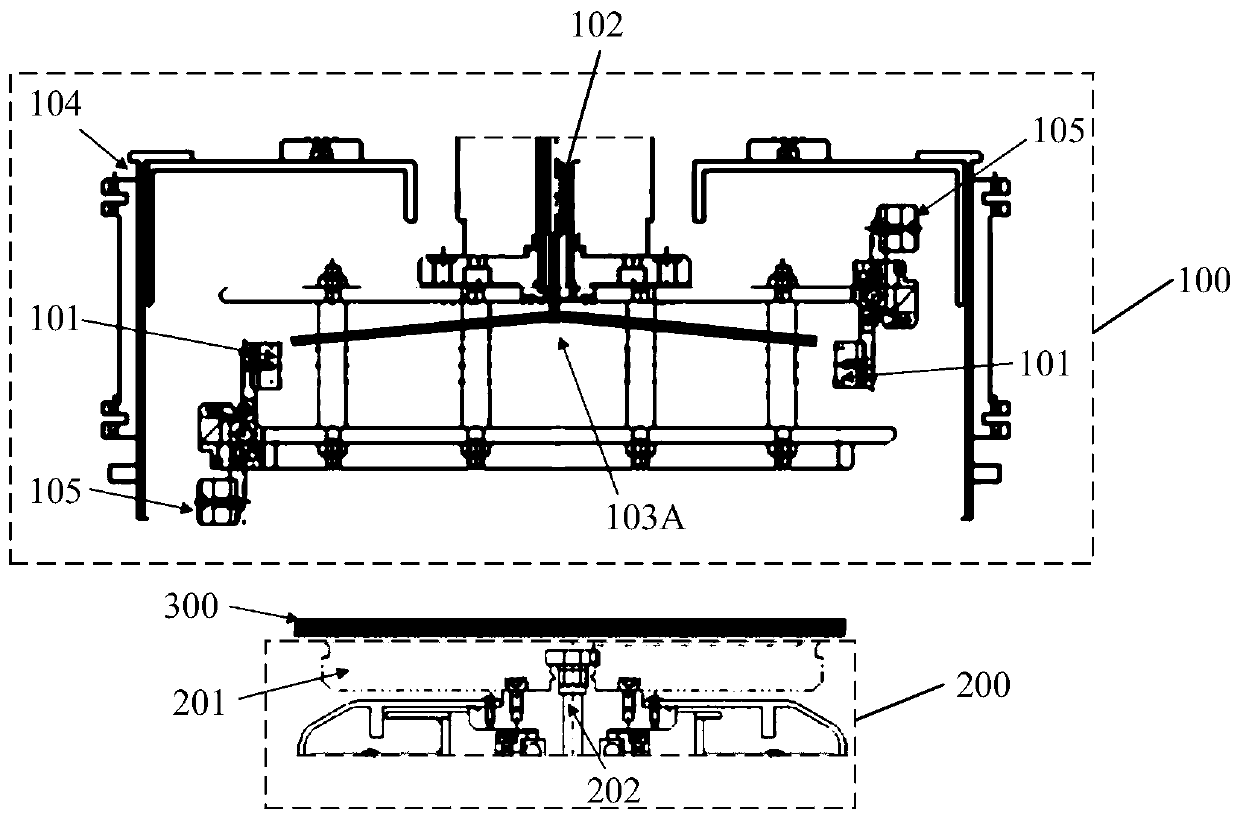
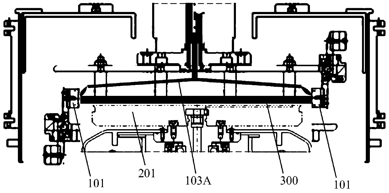
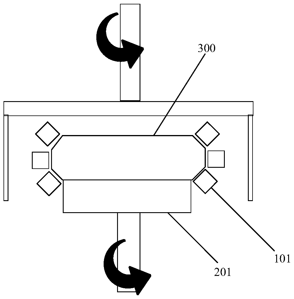
[0027] An embodiment of the present invention provides a wafer grinding assembly 100 .

[0028] Such as figure 1 As shown, the wafer grinding assembly 100 (Round head, or drum) is used to cooperate with the wafer holder 200 to complete the grinding (Grinding) of the edge (Edge) of the wafer 300 (Wafer), improving Edge roughness of the wafer 300 .

[0029] Such as figure 1 As shown, during implementation, the wafer 300 is fixed on the wafer holder 20...


PUM


Abstract

The invention provides a wafer grinding assembly and grinding equipment. The wafer grinding assembly includes a plurality of grinding pads, a liquid supply assembly and an adjusting assembly. The plurality of grinding pads are distributed annularly around the center of the wafer grinding assembly, the liquid supply assembly is used for providing grinding liquid, the adjusting assembly is arrangedby corresponding to a liquid outlet of the liquid supply assembly, the adjusting assembly extends from the center of the wafer grinding assembly to the direction close to the grinding pads, and the adjusting assembly is used for enabling the grinding liquid provided by the liquid supply assembly to drop from the side, close to the grinding pads, of the adjusting assembly. According to the embodiment of the invention, the adjusting assembly is arranged, when grinding liquid is supplied, the grinding liquid can directly drop on the edge of the ground wafer through the adjusting effect of the adjusting assembly, so that the grinding liquid is prevented from flowing through the upper surface of the wafer, the influence possibly caused by the grinding liquid on the upper surface of the wafer can be reduced, and the possibility that defects are generated on the surface of the wafer is reduced.

Description

technical field [0001] The invention relates to the technical field of semiconductor preparation, in particular to a wafer grinding assembly and grinding equipment. Background technique [0002] During semiconductor production and processing, it is necessary to coat (Coating) photoresist (PR for short), and defects near the edge of the semiconductor (Edge) may lead to uneven coating of PR. Grinding and edge polishing (Edge Polishing) of the wafer can reduce the possibility of cracking (Crack) on the wafer due to external factors such as impact. [0003] Wafers need to add edge slurry (edge ​​slurry) during the grinding process. The existing edge slurry addition process is to drop the slurry on the center of the wafer. In this way, during the rotation of the wafer around its own axis, the slurry is Centrifugal movement, moving from the upper surface of the wafer to the edge of the wafer, and flows between the wafer and the polishing pad. Generally speaking, the abrasive liq...

Claims


Application Information

Patent Timeline
IPC IPC(8): B24B37/00B24B37/11B24B37/27B24B57/02
CPCB24B37/00B24B37/11B24B37/27B24B57/02
Inventor 崔世勋
Owner XIAN ESWIN SILICON WAFER TECH CO LTD
Why Eureka
Try Eureka