Quasi-monocrystalline silicon crystal growth method and thermal field structure

A crystal growth, monocrystalline silicon-like technology, which is applied in the field of solar silicon materials, can solve the problems of increasing the cost of seed crystal use, high metal impurity content, and increased metal impurity content, and achieves reduced melting time, low crystal defect density, Avoid the effects of spreading contamination

Active Publication Date: 2019-09-06
常州常晶科技有限公司
View PDF7 Cites 3 Cited by
  • Summary
  • Abstract
  • Description
  • Claims
  • Application Information

AI Technical Summary

Problems solved by technology

[0006] However, there are also important deficiencies in the cast single crystal process: first, the seed crystal needs to be laid on the bottom of the crucible first, and undergoes the entire high-temperature melting process. Special control of the thermal field and process is required to avoid complete melting of the seed crystal, resulting in Seedless-induced crystal growth renders the cast monocrystalline silicon process completely ineffective
In order to suppress the internal growth of polycrystalline grains on the side wall of the crucible and destroy the integrity of the cast single crystal silicon crystal, the size of the crucible is usually enlarged to cut off this part of the crystal, which causes an additional loss in the yield of the final product
Fourth, due to the lack of grain boundaries of cast single crystal silicon crystals, and due to the large size of the crystal ingot, thermal stress is generated due to uneven temperature in the body, resulting in the generation of defects in the upper part of the crystal ingot and the rapid increase in value, which reduces the quality of cast single crystals and performance Even lower than ordinary polysilicon
Fifth, since the seed crystal has to go through a long process of melting and crystal growth, the thermal stress causes damage to the crystal structure of the seed crystal, and is affected by the diffusion of impurities from the silicon material and the crucible, and the content of metal impurities increases, resulting in a decline in the quality of the recovered seed crystal , is not conducive to the recycling of seed crystals, and increases the cost of using seed crystals
Sixth, the growth characteristic of the casting method is that the crystal is directional solidified from the bottom of the crucible from bottom to top. Due to segregation, the final solidified part of the top of the crystal ingot has a high content of metal impurities. During the subsequent cooling process of the crystal, the metal impurities diffuse back, Causes the low number of red areas on the head; the low number of red areas on the head, bottom, and sides are inherent defects in the directional growth of crystals in the crucible, resulting in a product pass rate of only 50% to 60%, which is lower than that of Cz single crystal
However, this invention, like the ordinary casting process, cannot improve the low-minority red zone at the head, side and tail of the crystal ingot caused by the diffusion of metal impurities, resulting in a loss of about 25% of the yield of the crystal ingot

Method used


Image

  • Quasi-monocrystalline silicon crystal growth method and thermal field structure
  • Quasi-monocrystalline silicon crystal growth method and thermal field structure
  • Quasi-monocrystalline silicon crystal growth method and thermal field structure

Examples


Embodiment 1

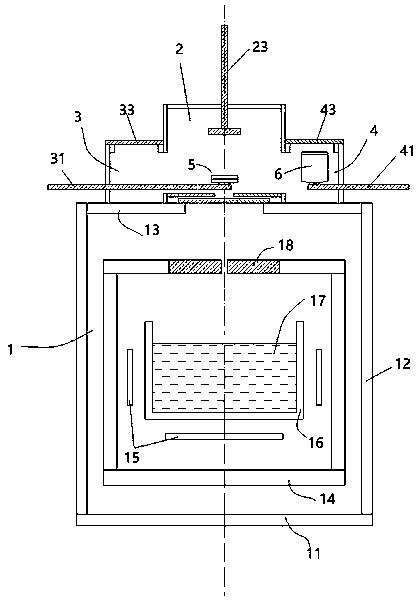
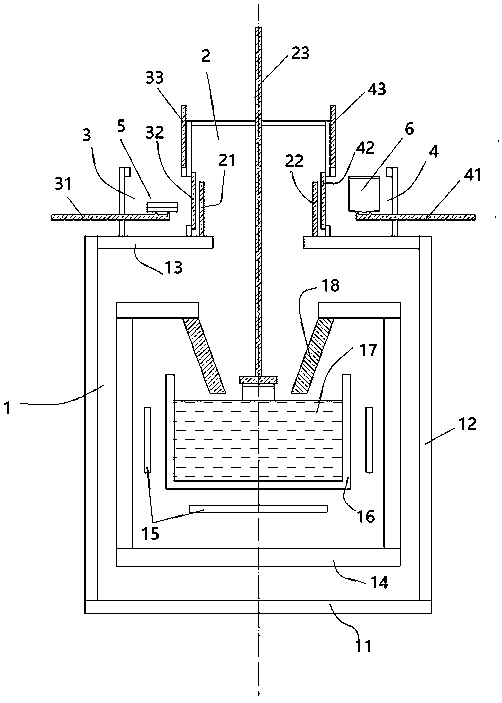
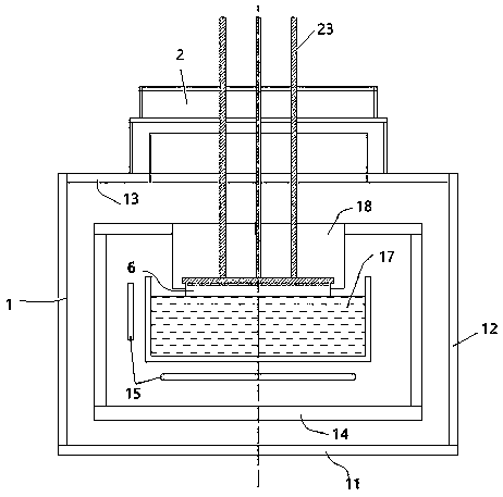
[0065] In order to match the subsequent ingot slicing equipment, the size of the seed crystal 51 is (length*width*thickness) 650mm*165mm*25mm, and the crystal orientation in the thickness direction is the direction. A polycrystalline high-purity crucible 16 purchased from the market is used, and 480 kg of silicon material is charged. The crucible 16 is connected to the furnace bottom 11 and can be opened for loading and unloading operations of the crucible 16 . After the crucible 16 is loaded into the main furnace chamber, the main furnace chamber 1 is closed, and the main furnace chamber 1 and the auxiliary furnace chamber 2 partition plates (21 and 22). The main furnace chamber 1 is vacuumed (atmospheric pressure less than 0.01mbar) and then heated, and a protective gas (argon) is introduced. The pressure in the furnace is 600mbar, and the gas flow rate is 50SLPM. The insulation board 18 is set to a horizontal state, such as figure 2 Shown, in order to reduce the heat lo...

Embodiment 2

[0076] Using the same production process as that of Example 1, the size of the seed crystal 51 is (length*width*thickness) 900mm*165mm*25mm, and the charge amount is 510kg. Since the ingot only becomes longer and the width remains unchanged, the crystal growth rate remains unchanged. The weight of a single crystal rod is about 60kg, and the weight of the rear rod (size: 159mm*159mm*900mm) is about 53kg. Eight times of growth are carried out with one feeding, the melting time of silicon material is 10 hours, and the total cycle is 42 hours. Each seed crystal is recycled 2 to 3 times, and a total of 3 new seed crystals are used, each seed crystal is 8.65kg, and the total weight is 26kg. Then the effective output of the final square rod is 424kg, the total input of silicon material is 536kg, and the qualified rate of output is 79%. The 24-hour square rod output of a single device is 242kg, and the monthly (30 days) output is 7260kg.

Embodiment 3

[0078] Adopt the same technological process as embodiment 1. In order to increase the output per unit time, a seed crystal with a size of 650mm*330mm*25mm is used, the weight of a single block is 12.5kg, and the loading capacity is 800kg. As the ingot becomes wider, the growth rate decreases, and the growth cycle of the single crystal ingot is increased to 5 hours. The weight of a single ingot is about 85kg, and two square ingots with a size of 159mm*159mm*650mm can be produced at one time, with a total weight of about 76.6kg. 9 times of growth are carried out with one feeding, the melting time of silicon material is 15 hours, and the total cycle is 60 hours.

[0079] Each seed crystal is recycled 2 to 3 times, and a total of 4 new seed crystals are used, with a weight of 50 kg. Then the final square bar output is 690kg, the total silicon material input is 850kg, and the pass rate of the product (square bar) is 81%. The 24-hour square rod output of a single device is 276kg,...


PUM

PropertyMeasurementUnit
lengthaaaaaaaaaa
thicknessaaaaaaaaaa
lengthaaaaaaaaaa

Abstract

The invention discloses a quasi-monocrystalline silicon crystal growth method and a thermal field structure, and relates to the technical field of solar crystalline silicon materials. Single platy seed crystals are used, and under seed crystal induction, a quasi-square crystal with the height slightly equal to the width grows from silicon melt in the seed crystal thickness direction from top to bottom. In order to implement the crystal growth method, the thermal field structure comprises a main furnace room, an auxiliary furnace room, a seed crystal loading cavity, a crystal bar unloading cavity, a crystal listing mechanism, a crucible, a heater, a heat preservation basket, a heat insulation board and the like; the crystal lifting mechanism in the auxiliary furnace room mounts the seed crystals to induce crystal growth; in the crystal growth process, seed crystal module preparation and crystal bar taking are conducted in the crystal loading cavity and the crystal bar unloading cavity,after crystal bar growth is completed, the crystal lifting mechanism can rapidly unload and re-mount a seed crystal block to grow the next crystal. The grown quasi-monocrystalline crystal has the advantages of being uniform in crystal orientation, low in edge leather ratio, high in product qualification ratio, low in defect density and high in production efficiency.

Description

technical field [0001] The invention relates to the technical field of solar silicon materials, in particular to a method for growing silicon-like crystals and a thermal field structure. Background technique [0002] Solar photovoltaic power generation is the main way of solar photovoltaic application because of its environmental friendliness, high conversion efficiency, and convenient installation. In the past ten years, the cost of photovoltaic power generation has dropped rapidly to the on-grid electricity price close to that of traditional thermal power, which provides strong support for the further large-scale application of photovoltaic power generation. [0003] Monocrystalline silicon wafers and polycrystalline silicon wafers are two basic materials for making photovoltaic cells. Monocrystalline silicon wafers are grown and cut by pulling (Cz) crystals. They are characterized by less defects, high minority carrier life, and stable quality, so they are favored by hig...

Claims


Application Information

Patent Timeline
Patent Type & Authority Applications(China)
IPC IPC(8): C30B15/00C30B15/36C30B15/14C30B29/06
CPCC30B15/00C30B15/14C30B15/36C30B29/06
Inventor 张志强
Owner 常州常晶科技有限公司
Why Eureka
Try Eureka