Device and method for measuring secondary electron emission coefficient of material
A technology of secondary electron emission and coefficient, applied in the fields of physical electronics and optoelectronics
- Summary
- Abstract
- Description
- Claims
- Application Information
AI Technical Summary
Problems solved by technology
Method used
Image
Examples
Embodiment 1
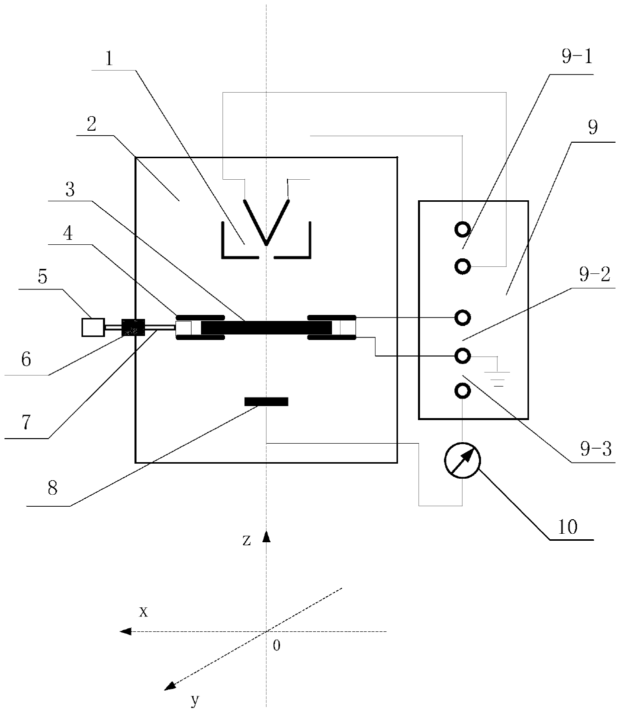
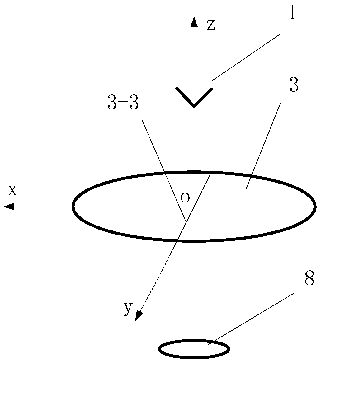
[0038] Such as figure 1 As shown, a device for measuring the secondary electron emission coefficient of materials, including an electron gun 1, a microchannel plate 3, a test fixture 4, a manipulator 5, a bellows 6, a moving guide rod 7, a collector 8, an ammeter 10, and a vacuum chamber 2 And working power source 9, it is characterized in that: in vacuum chamber 2 along the central axis z of vacuum chamber 2, electron gun 1, test fixture 4 and collector 8 that are arranged in parallel successively from top to bottom; Test fixture 4 is equipped with microchannel plate 3. The micro-channel plate adopts the Φ25-6 / 8 type micro-channel plate used by the intensifier. The micro-channel plate 3 includes the input end 3-4 and the output end 3-5. The input end 3-4 of the micro-channel plate faces the electron gun 1. Both the input end 3-4 and the output end 3-5 are plated with nickel-chromium electrodes, wherein the nickel composition is 80%, the chromium composition is 20%, and the p...
Embodiment 2
[0048] Measuring SiO 2 Secondary electron emission coefficients of materials bombarded with different electron energies
[0049] The micro-channel plate adopts the Φ25-6 / 8 type micro-channel plate used in the image intensifier, its diameter is Φ25mm, the channel aperture is 6μm, the channel center distance is 8μm, the plate thickness is 0.3mm, and the input and output electrodes are nickel-chromium alloy, wherein the nickel composition is 80%, the chromium composition is 20%, and the purity is 99.9%.
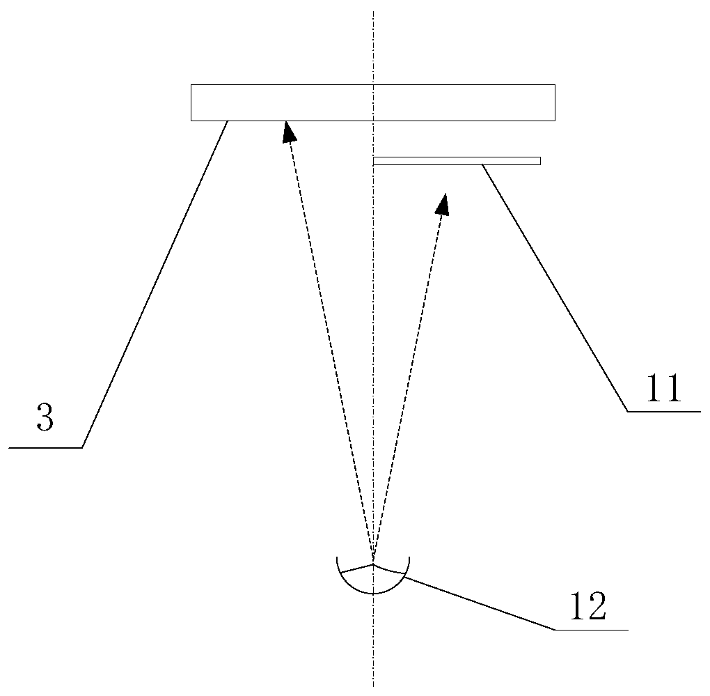
[0050] Evaporation source 12 is SiO 2 Materials, put the microchannel plate into the vacuum coating machine, and plate a layer of SiO with a thickness of 250nm on the input end of the microchannel plate according to the usual coating process. 2 film layer. The microchannel plate is then placed on the test fixture of the measurement device so that it makes good contact with the input and output electrodes on the test fixture. Adjust the position of the micro-channel plate so ...
PUM
| Property | Measurement | Unit |
|---|---|---|
| Diameter | aaaaa | aaaaa |
| Diameter | aaaaa | aaaaa |
| Thickness | aaaaa | aaaaa |
Abstract
Description
Claims
Application Information


