Wiring repair method, array substrate and display panel
An array substrate and wiring technology, applied in the field of liquid crystal display, can solve the problems of leakage and electrical connection of data lines and storage capacitor lines, and achieve the effect of ensuring normal transmission
- Summary
- Abstract
- Description
- Claims
- Application Information
AI Technical Summary
Problems solved by technology
Method used
Image
Examples
Embodiment 1
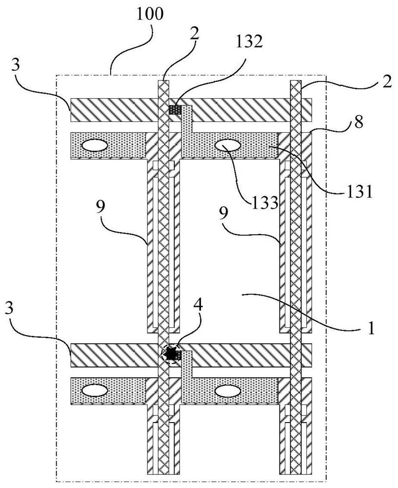
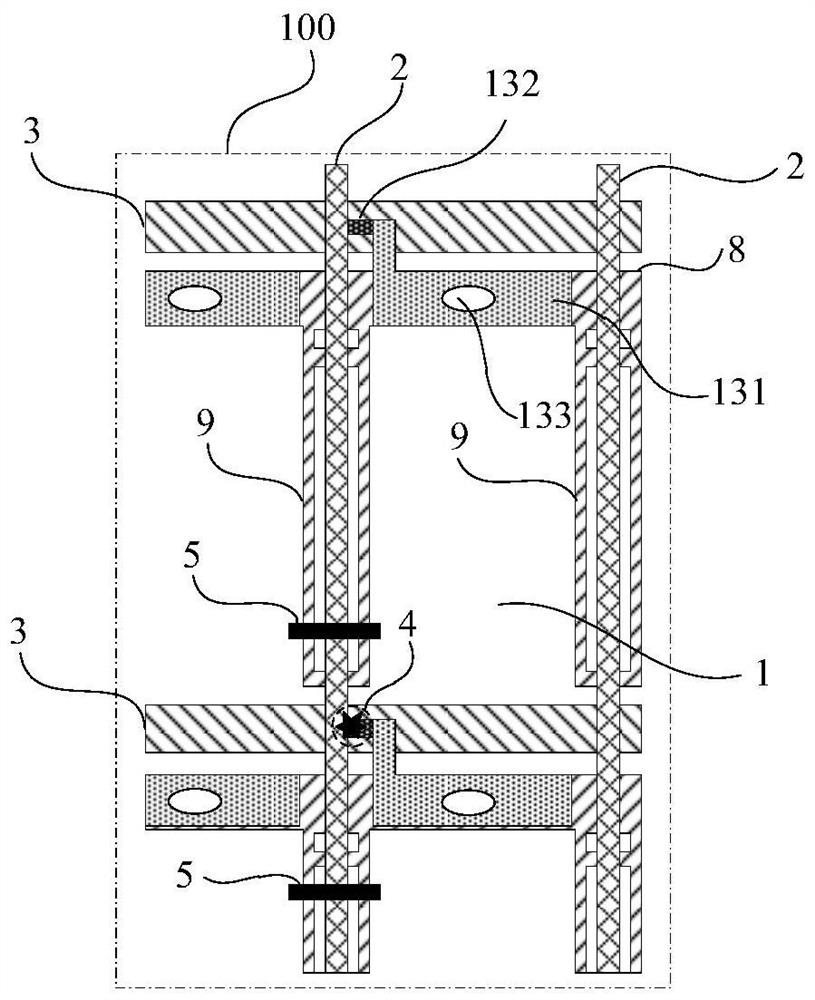
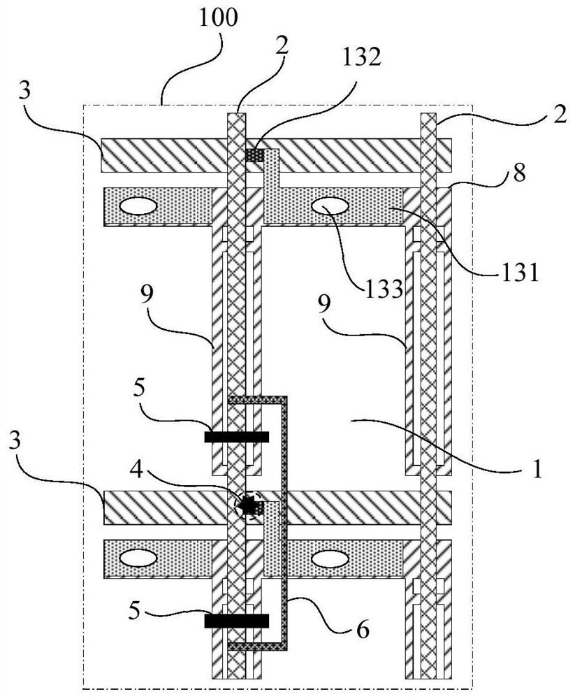
[0031] Figure 4 It is a schematic diagram of a partial structure of an array substrate in the prior art. Below to Figure 4 The shown back channel etched array substrate 100 is taken as an example, combined with Figure 1 to Figure 3 The basic structure of the array substrate 100 is introduced as shown. Of course, the array substrate 100 mentioned in the present invention is not limited thereto, and may also be of other types. Furthermore, it should be understood that Figure 1 to Figure 3 Only a part of the array substrate 100 is shown in the figure, and a complete pixel area 1 of the array substrate 100 and a part of the structure around the pixel area 1 are shown in detail. In practical applications, the pixel area 1 of the array substrate 100 includes multiple The pixel area 1 , and according to the size of the liquid crystal display, that is, the performance requirement, the pixel area 1 of different liquid crystal displays may include different numbers of pixel areas...
Embodiment 2
[0066] This embodiment provides an array substrate 100, which is an array substrate 100 corresponding to the wiring repair method described in Embodiment 1, that is, the wiring repair method described in Embodiment 1 is specifically for the array described in this embodiment Substrate 100 is repaired.
[0067] The array substrate 100 of this embodiment includes data lines 20, scan lines 30, storage capacitor bus lines 80, and storage capacitor branch lines 90. The data lines 20 and scan lines 30 are arranged in a criss-cross pattern to define the pixel area 10, the storage capacitor bus lines 80 and the scan lines. The lines 30 are arranged in parallel; the storage capacitor branch line 90 includes a first branch line 91 and a second branch line 92 located in the same pixel area 10, the first branch line 91 is adjacent to the projection direction of the data line 20, and the first branch line 91 is connected to Between the storage capacitor bus 80 and the second segment of the...
Embodiment 3
[0079] This embodiment provides a repaired array substrate 100, the structure of the repaired array substrate 100 provided in this embodiment corresponds to the structure of the array substrate 100 provided in Embodiment 2, and the repaired array substrate 100 of this embodiment 100 is the array substrate 100 after the array substrate 100 described in the second embodiment is repaired by the wiring repair method described in the first embodiment.
[0080] The repaired array substrate 100 provided in this embodiment includes data lines 20, scan lines 30, storage capacitor bus lines 80, storage capacitor branch lines 90, and repair lines 60. The data lines 20 and scan lines 30 are arranged in a criss-cross pattern and define pixel areas. 10. The storage capacitor bus 80 and the scanning line 30 are arranged in parallel; the storage capacitor branch line 90 includes a first branch line 91 and a second branch line 92 located in the same pixel area 10, and the first branch line 91 i...
PUM
 Abstract
Description
Claims
Application Information


