High-frequency polishing quartz wafer with bump structure

A technology of quartz wafers and bumps, which is applied in the field of communication, and can solve problems such as chip damage, chip stacking, and large crystal resonator DLD2 parameters.

Pending Publication Date: 2019-09-10
CHENGDU TIMEMAKER CRYSTAL TECH
View PDF0 Cites 0 Cited by
  • Summary
  • Abstract
  • Description
  • Claims
  • Application Information

AI Technical Summary

Problems solved by technology

[0003] As the wafer becomes thinner and thinner, its surface roughness is low, resulting in lamination of the wafer during the cleaning process
Once the two wafers are stacked together, a vacuum area appears due to the very smooth surface, resulting in the overlapping area cannot be cleaned, resulting in excessive crystal resonator DLD2 (level-dependent characteristics) parameters; if forcibly separated, the wafer will be damaged

Method used


Image

  • High-frequency polishing quartz wafer with bump structure
  • High-frequency polishing quartz wafer with bump structure
  • High-frequency polishing quartz wafer with bump structure

Examples


Embodiment 1

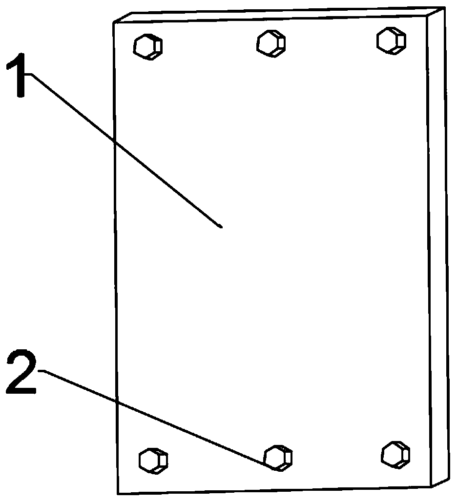
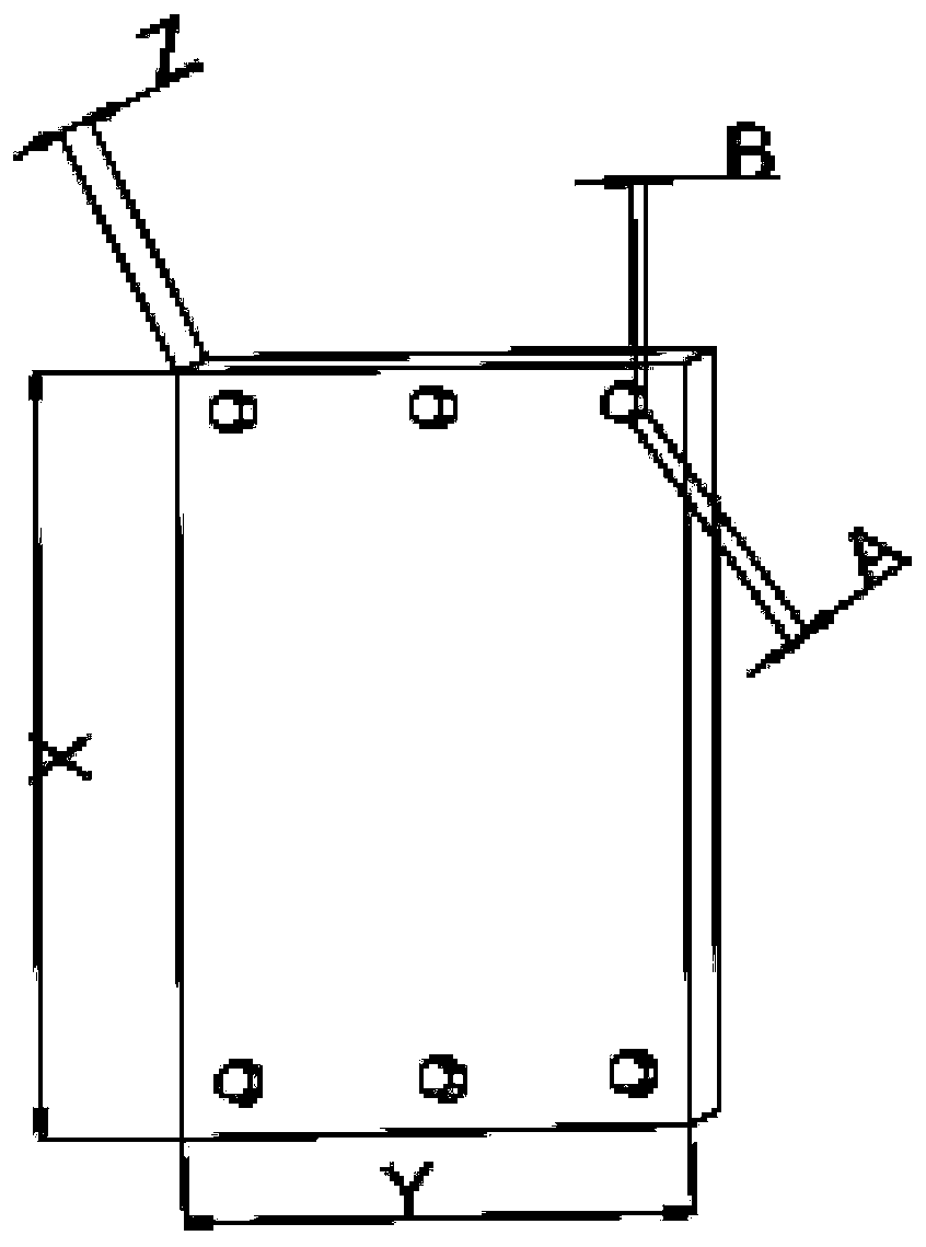
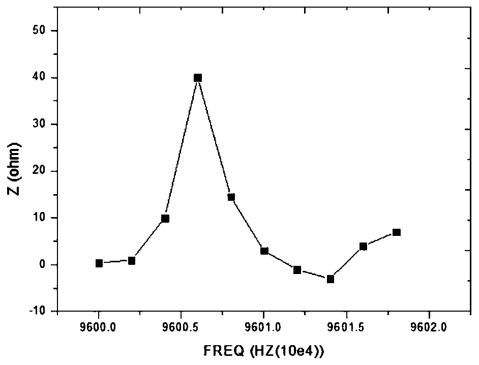
[0036] A high-frequency polished quartz wafer with a bump structure provided by a preferred embodiment of the present invention, the original wafer of a rectangular wafer, when the length, width and height of the rectangular wafer 1 are respectively 1.35mm, 0.93mm and 0.017mm, the ANSYS finite element software adopted, The amplitude-frequency characteristics and impedance characteristics of the crystal vibration of the original wafer under the excitation of the alternating electric field are calculated through harmonic response analysis; the impedance value is obtained as 40Ω.

Embodiment 2

[0038] This embodiment is based on the first embodiment, when the number of bumps 2 is eight. Both the length A and the height B of the bump are variable, and the unit is mm. Through the ANSYS finite element software, the harmonic response analysis is used to calculate the amplitude-frequency characteristics and impedance characteristics of the crystal vibration of the prismatic quartz wafer under the excitation of the alternating electric field; get table 1

[0039] Table 1

[0040]

[0041] As can be drawn from Table 1, the size of the bump 2 is as shown above, and the impedance value when 8 bumps 2 are set on the rectangular wafer 1 is as shown above, compared with the impedance value of the original wafer; it can be found that as the bump height B The increase of the size means that the length / width ratio of the overall structure size of the prism quartz wafer decreases, and the load at the end increases, which inhibits the crystal vibration, so its impedance will incr...

Embodiment 3

[0043]This embodiment is based on the first embodiment, when the number of bumps 2 is twelve. Both the length A and the height B of the bump are variable, and the unit is mm. Through the ANSYS finite element software, the harmonic response analysis is used to calculate the amplitude-frequency characteristics and impedance characteristics of the crystal vibration of the prismatic quartz wafer under the excitation of the alternating electric field; get table 2

[0044] Table 2

[0045]

[0046] From Table 2, it can be drawn that the size of the bump 2 is as shown above, and the impedance value when 12 bumps 2 are set on the rectangular wafer 1 is as shown above, compared with the impedance value of the original wafer; it can be found that with the bump height B The increase in the size of the prismatic quartz wafer means that the length / width ratio of the overall structure size of the prism quartz wafer decreases and the load on the end increases, which inhibits the crystal ...


PUM

PropertyMeasurementUnit
Length and widthaaaaaaaaaa

Abstract

The invention discloses a high-frequency polished quartz wafer with a bump structure, which comprises a rectangular wafer with lengths, widths and heights of X, Y and Z. Prismatic bumps are arranged on the upper surface and the lower surface of the rectangular wafer in a mirroring manner, and the bumps are positioned at opposite angles of the surface where the bumps are positioned; the edge lengthof the bump is A, and the height of the bump is B; wherein B is greater than or equal to 0.06Z and less than or equal to 0.24Z; and 0.01Y<=A<=0.03Y. In order to overcome the defects in the prior art,the invention designs a quartz wafer with a convex structure. The traditional thought of wafer manufacturing and cognition is broken through; the problems in the background technology are solved; wherein the rectangular wafer is an original wafer, is not unique in size, and is mainly suitable for the size specification of the wafer from a large-size SMD7050 specification to a small-size SMD1210 specification. According to the scheme, the corresponding small cylinders are etched on the surface of the wafer in a photoetching mode to prevent lamination.

Description

technical field [0001] The invention belongs to the communication field and relates to a high-frequency polished quartz wafer with a bump structure. Background technique [0002] With the development of 5G communication, the wavelength of communication is getting shorter and shorter, and its communication frequency is getting higher and higher accordingly; the core component of an AT-cut quartz crystal resonator or oscillator is a piezoelectric quartz crystal frequency plate, and its thickness is the same as The resonant frequency satisfies: t=1664 / f (wherein t represents the thickness of wafer; f represents the frequency of wafer), can be clearly opened to along with the increase of the resonant frequency of wafer by this formula, the thickness of wafer becomes more and more correspondingly Thin. In addition, in order to reduce the impedance of the high-frequency quartz wafer, it is often achieved by changing the surface roughness of the wafer to reduce its resonance dampi...

Claims


Application Information

Patent Timeline
IPC IPC(8): H03H9/19
CPCH03H9/19
Inventor 李辉叶竹之
Owner CHENGDU TIMEMAKER CRYSTAL TECH
Why Eureka
Try Eureka