LED chip and manufacturing method thereof

A technology of LED chips and electrodes, which is applied in the direction of electrical components, circuits, semiconductor devices, etc., can solve the problems of no light-emitting area and light loss in the N-type electrode area, improve luminous efficiency and luminous brightness, avoid leakage, and improve current expansion effect of effect

Pending Publication Date: 2019-09-13
XIAMEN QIANZHAO SEMICON TECH CO LTD
View PDF0 Cites 2 Cited by
  • Summary
  • Abstract
  • Description
  • Claims
  • Application Information

AI Technical Summary

Problems solved by technology

Specifically, the electrode is formed of a pad and a metal electrode extension, and the electrode extension of the electrode pad absorbs light generated in the active layer, thereby causing light loss, and the N-type electrode region has no light emitting area

Method used


Image

  • LED chip and manufacturing method thereof
  • LED chip and manufacturing method thereof
  • LED chip and manufacturing method thereof

Examples


Embodiment Construction

[0045] In order to make the content of the present invention clearer, the content of the present invention will be further described below in conjunction with the accompanying drawings. The invention is not limited to this specific example. Based on the embodiments of the present invention, all other embodiments obtained by persons of ordinary skill in the art without making creative efforts belong to the protection scope of the present invention.

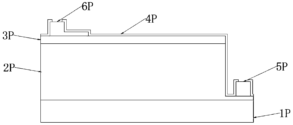
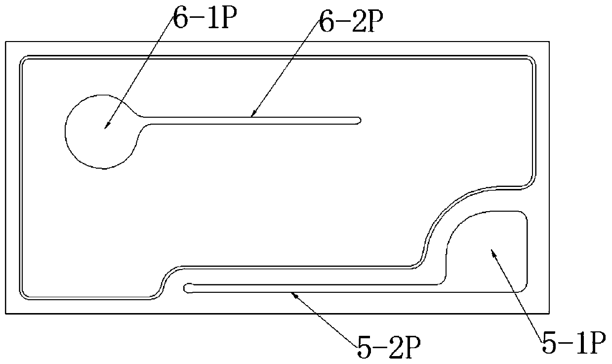
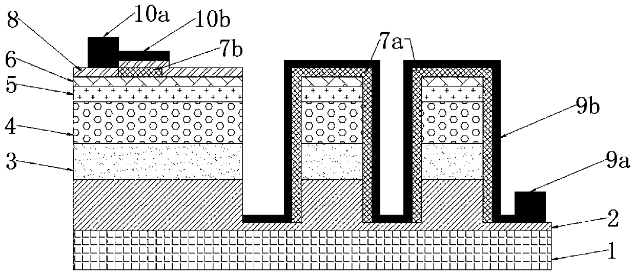
[0046] The LED chip provided by this embodiment, such as Figure 3-Figure 5 shown, including:

[0047] substrate1;

[0048] The epitaxial layer structure arranged on the surface of the substrate 1; the epitaxial layer structure includes: N-type semiconductor layer 2, active region 3, P-type semiconductor layer 4, highly doped P-type semiconductor layer 5, high Doped tunneling layer 6;

[0049] The surface of the epitaxial layer structure away from the substrate includes an N electrode fabrication area and a P electrode fabricat...


PUM


Abstract

The invention provides an LED chip and a manufacturing method thereof. The epitaxial layer structure of the LED chip comprises: an N-type semiconductor layer, an active region, a P-type semiconductorlayer, a high-doped P-type semiconductor layer and a high-doped tunneling layer which are sequentially overlapped on the substrate. The manufacturing method of the LED chip comprises the steps of: firstly, forming a plurality of light-emitting columns in the N electrode manufacturing area of the epitaxial layer structure, so that the light-emitting area of the LED chip is increased; secondly, arranging a first insulating reflecting layer which comprises an insulating layer and a reflecting layer, wherein the reflecting layer is stacked on the surface of the insulating layer, so that the insulating layer is directly in contact with the high-doped tunneling layer, and lattice matching is performed on the high-doped tunneling layer and the insulating layer to form stress transition, thereby improving the combination degree of the first insulating reflecting layer and the epitaxial layer structure; and finally, insulating an N-type electrode extension strip from a light emitting area through the first insulating reflecting layer, so that the electric leakage of the LED chip can be effectively avoided.

Description

technical field [0001] The invention belongs to the field of light-emitting diodes, and more specifically relates to an LED chip and a manufacturing method thereof. Background technique [0002] Due to the advantages of high brightness, small size and low power consumption of light emitting diodes (Light Emitting Diode, LED), light emitting diodes are regarded as a new generation of lighting tools, and in recent years, light emitting diodes have also been used in more fields Rapid adoption and popularity. However, because the existing semiconductor chips of light-emitting diodes still have the problem of low luminous efficiency, how to improve the luminous efficiency of semiconductor chips of light-emitting diodes has become one of the most important topics in the field of scientific research today. [0003] attached figure 1 shows the structural diagram of the existing semiconductor chip, attached figure 2 shows a top view of the existing semiconductor chip, in figure ...

Claims


Application Information

Patent Timeline
Patent Type & Authority Applications(China)
IPC IPC(8): H01L33/24H01L33/38H01L33/46H01L33/14H01L33/00
CPCH01L33/005H01L33/14H01L33/24H01L33/385H01L33/46H01L2933/0016H01L2933/0025
Inventor 李镇勇林志伟尤翠萍罗桂兰
Owner XIAMEN QIANZHAO SEMICON TECH CO LTD
Why Eureka
Try Eureka