Printed circuit board, manufacturing method thereof, and method for printing mark thereon

A technology for printed circuit boards and manufacturing methods, which are applied in printed circuit components, circuit inspection/recognition, conductive pattern formation, etc., can solve problems such as unclear marks, oily marks, and surfaces that are easily rubbed and bumped.

Inactive Publication Date: 2019-09-17
江门荣信电路板有限公司
View PDF5 Cites 0 Cited by
  • Summary
  • Abstract
  • Description
  • Claims
  • Application Information

AI Technical Summary

Problems solved by technology

Since the logo is printed on the surface, the surface is susceptible to friction and bumps during production and use, and there is a risk of the logo losing oil, resulting in unclear logos

Method used


Image

  • Printed circuit board, manufacturing method thereof, and method for printing mark thereon

Examples


Embodiment 1

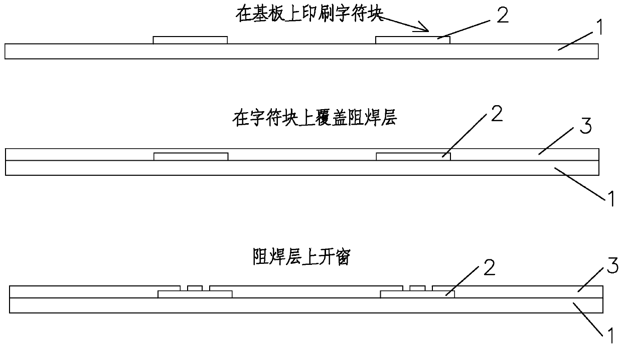
[0028] A method for printing a mark on a printed circuit board, comprising the following steps:

[0029] Step 1) Select the substrate 1 as a glass fiber substrate, and silk-screen character blocks 2 on the glass fiber substrate. The character blocks 2 are solid and non-transparent in color, and the character blocks 2 are larger than the outline of the above-mentioned logo. In this embodiment, a glass fiber substrate is used. The glass fiber substrate uses epoxy resin as an adhesive and glass fiber cloth as a reinforcing material; the glass fiber substrate can adapt to a higher working temperature and is less affected by the environment, so silk screen The character block 2 above it can have more ink options, and both photosensitive ink and UV ink can be used. The color of the character block 2 is not limited. In this implementation, as one of the preferred options, black photosensitive ink is selected. The photosensitive ink has the advantages of easy acquisition and economic ...

Embodiment 2

[0033] A method for printing a mark on a printed circuit board, comprising the following steps:

[0034] Step 1) In this embodiment, the substrate 1 is selected as a paper substrate, and the character block 2 is silk-screened on the paper substrate. The character block 2 is a solid non-transparent black block, and the character block 2 is larger than the outline of the above-mentioned logo. In this embodiment Among them, the character block 2 is designed to be 0.5mm larger than one side of the logo. The characters use black UV ink, and the curing process adopts UV curing, and the UV energy is 1600-2200mj.

[0035] In this embodiment, a paper substrate is used. The paper substrate has the characteristics of being capable of punching, low cost, low price, and low relative density. For example, in this embodiment, an easily available FR-2 paper substrate is used.

[0036] Step 2) On the character block 2 made of cured black UV ink, apply white UV solder resist as the solder resi...

Embodiment 3

[0039] A method for printing a mark on a printed circuit board, comprising the following steps:

[0040] Step 1) select the substrate 1 as a paper substrate, and screen-print a character block 2 on the paper substrate. The character block 2 is a solid non-transparent black block, and the character block 2 is larger than the outline of the above-mentioned logo. In this embodiment, the character block 2 The design is 0.5mm larger than the one side of the logo. The character block 2 is screen-printed with black UV ink, and the curing process adopts UV curing, and the UV energy is 1600-2200mj.

[0041] In this embodiment, a paper substrate is used. The paper substrate has the characteristics of being capable of punching, low cost, low price, and low relative density. For example, in this embodiment, an easily available FR-2 paper substrate is used.

[0042] Step 2) Apply white solder resist photosensitive oil on the black character block 2 made of cured black UV ink as the solder...


PUM


Abstract

The invention provides a method for printing a mark on a printed circuit board. The method comprises the steps of printing an opaque character block on a substrate, wherein the character block is larger than the profile of the mark; covering the character block with an opaque solder resist layer, wherein the solder resist layer and the character block have a color contrast or contrast characteristic; disposing a window on the solder resist layer for the mark; exposing the character block through the window portion of the solder resist layer to form the shape of the mark. The method prevents the mark form residing at the surface of the printed circuit board so as to greatly reduce the friction probability of the mark and reduce the risk that the mark is de-oiled and is not clear. The invention also provides a printed circuit board manufacturing method which comprises the method for printing the mark, and a printed circuit board manufactured by using the printed circuit board manufacturing method.

Description

technical field [0001] The invention relates to the field of manufacturing printed circuit boards, in particular to a printed circuit board, a manufacturing method thereof, and a method for printing marks on the printed circuit board. Background technique [0002] In the production process of printed circuit boards, in order to better identify the basic information of printed circuit boards, it is often necessary to print some marks on printed circuit boards, these marks include but are not limited to the production date of printed circuit boards, basic configuration parameters, welding position marks, etc. [0003] The existing method of printing logo on printed circuit board is: use the prepared graphic screen to force the ink to seep out from the mesh in the screen under the action of pressure, so that the logo can be missed on the surface of the printed circuit board . Since the logo is printed on the surface, the surface is susceptible to friction and bumps during pro...

Claims


Application Information

Patent Timeline
IPC IPC(8): H05K1/02H05K3/12
CPCH05K1/0266H05K3/12
Inventor 曾建华
Owner 江门荣信电路板有限公司
Why Eureka
Try Eureka