OLED display substrate and preparation method thereof and display device

A display substrate and base technology, which is applied in semiconductor/solid-state device manufacturing, organic semiconductor devices, electric solid-state devices, etc., can solve the problems of OLED display packaging reliability, cracking, and warping of inorganic layers, so as to improve packaging quality and display quality, and the effect of ensuring package reliability

Active Publication Date: 2019-09-20
BOE TECH GRP CO LTD +1
View PDF6 Cites 15 Cited by
  • Summary
  • Abstract
  • Description
  • Claims
  • Application Information

AI Technical Summary

Problems solved by technology

[0004] The above-mentioned EL scheme of removing the corresponding area of ​​the camera by laser cutting will cause the inorganic layer under the EL to ...

Method used


Image

  • OLED display substrate and preparation method thereof and display device
  • OLED display substrate and preparation method thereof and display device
  • OLED display substrate and preparation method thereof and display device

Examples


Embodiment 1

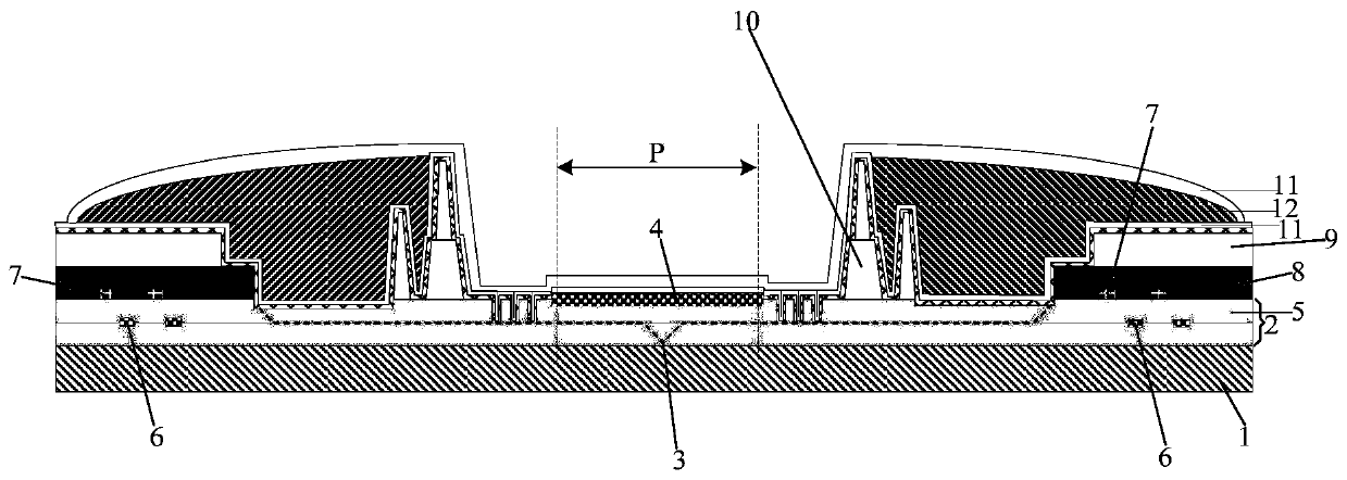
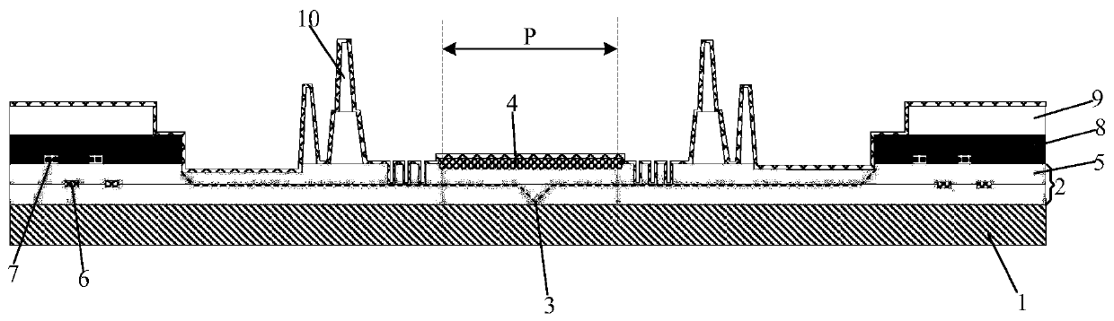
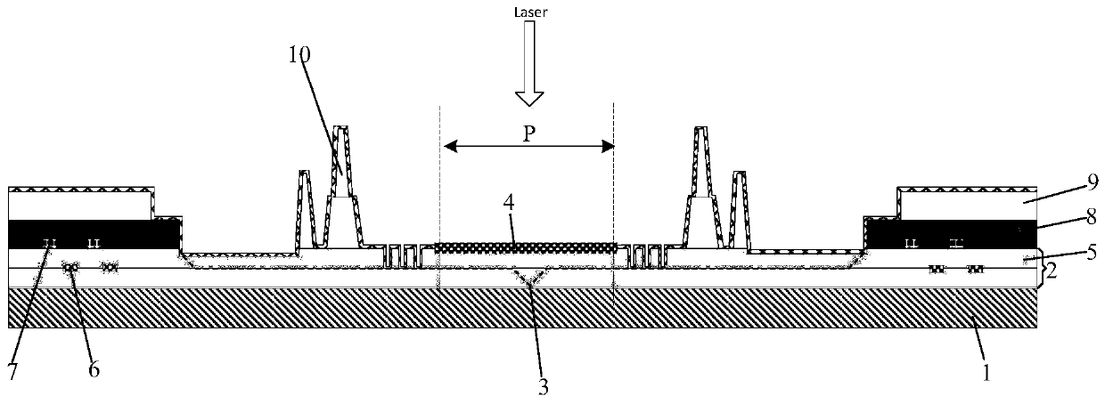
[0037] This embodiment provides an OLED display substrate, such as figure 1 As shown, it includes a base 1, an inorganic layer 2 and a light emitting unit 3 disposed on the base 1, the light emitting unit 3 is located on the side of the inorganic layer 2 away from the base 1, and the side of the base 1 away from the inorganic layer 2 is used to set the camera, the camera The orthographic projection area P on the substrate 1 is in the area where the light-emitting unit 3 is located, and the light-emitting unit 3 is not retained in the orthographic projection area P. The light-emitting unit 3 includes a light-emitting structure, in the orthographic projection area P, and away from the substrate 1 on the inorganic layer 2 One side is provided with a protective layer 4, and the protective layer 4 can protect the inorganic layer 2 in the orthographic projection area P when the light-emitting structure in the orthographic projection area P is removed by laser cutting, so as to preven...

Embodiment 2

[0071] This embodiment provides a display device, including the OLED display substrate in Embodiment 1.

[0072] By adopting the OLED display substrate in Embodiment 1, the encapsulation quality and display quality of the display device are improved.


PUM

PropertyMeasurementUnit
Thicknessaaaaaaaaaa

Abstract

The invention provides an OLED display substrate and a preparation method thereof and a display device. The OLED display substrate comprises a base, an inorganic layer arranged on the base and a light-emitting unit. The light-emitting unit is arranged on one side, away from the base, of the inorganic layer; one side, away from the inorganic layer, of the base is provided with a camera; and the orthographic projection area of the camera on the base is within the area of the light-emitting unit, and no light-emitting unit is retained in the orthographic projection area. The light-emitting unit comprises a light-emitting structure. A protection layer is arranged in the orthographic projection area and at the side, away from the base, of the inorganic layer. The protection layer can protect the inorganic layer in the orthographic projection area when the light-emitting structure in the orthographic projection area is removed through laser cutting to prevent the inorganic layer in the orthographic projection area from warping and cracking.

Description

technical field [0001] The invention belongs to the field of display technology, and in particular relates to an OLED display substrate, a preparation method thereof, and a display device. Background technique [0002] Organic Light Emitting Diode (OLED) has the advantages of self-illumination, wide viewing angle, bright color and ultra-thin flexibility, etc., and is widely used in the display field. At present, with the development of technologies such as narrow borders, the screen ratio of OLED is getting higher and higher, and it is expected to realize true full-screen technology. [0003] In order to realize the real full-screen technology, the camera technology under the screen came into being. The camera under the screen requires relatively high transmittance of the display screen, otherwise the resolution of the photos taken is not high. The organic light-emitting functional layer EL and other thick organic layers (such as pixel definition layer PDL, spacer PS, orga...

Claims


Application Information

Patent Timeline
IPC IPC(8): H01L27/32H01L51/52H01L51/56
CPCH10K59/65H10K59/10H10K50/11H10K50/80H10K50/805H10K50/84H10K2102/00H10K2102/302H10K71/00Y02E10/549H10K59/124H10K50/844H10K2102/311H10K59/122H10K77/111H10K2102/351
Inventor 杨璐史大为王文涛段岑鸿王培李旭黄灿吴帮炜
Owner BOE TECH GRP CO LTD
Why Eureka
Try Eureka