A kind of spatial optical waveguide preparation method

A space optical and optical waveguide technology, applied in the field of optical communication, can solve the problems of high connection loss, inability to realize low-loss connection of chip integrated optical waveguide, etc., to achieve the effect of reducing loss, eliminating alignment process, and realizing fast bridging

Active Publication Date: 2021-08-24
YANTAI MAGIC NANOTECHNOLOGY CO LTD
View PDF6 Cites 0 Cited by
  • Summary
  • Abstract
  • Description
  • Claims
  • Application Information

AI Technical Summary

Problems solved by technology

[0004] The existing technology uses optical fiber to realize the connection between two chip-integrated optical waveguides. The size of the optical opening on the chip integration is less than 1 micron (the optical opening refers to the connection section of the optical waveguide on the carrier), and the core diameter of the single-mode optical fiber is about 8-10 microns, the direct connection loss is as high as more than 99%. Usually, a coupler is used to match the chip optical waveguide mode spot with the fiber mode spot. Even in this way, the coupling connection loss is higher than 50%. The existing technical solutions cannot realize chip integration. Low-loss connection between optical waveguides

Method used


Image

  • A kind of spatial optical waveguide preparation method
  • A kind of spatial optical waveguide preparation method
  • A kind of spatial optical waveguide preparation method

Examples


Embodiment Construction

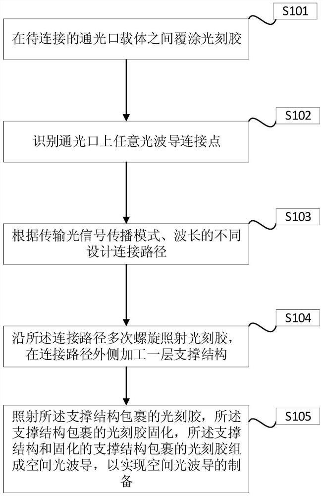
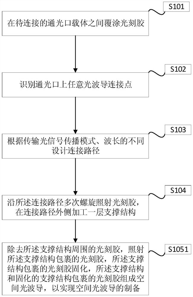
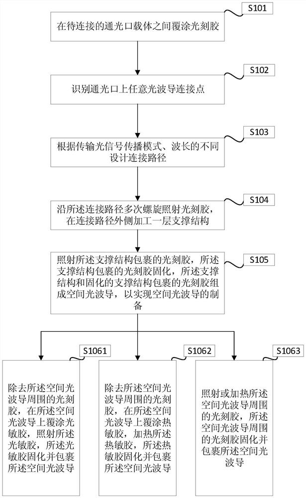
[0038] The following will clearly and completely describe the technical solutions in the embodiments of the application with reference to the drawings in the embodiments of the application. Apparently, the described embodiments are only some of the embodiments of the application, not all of them. Based on the embodiments in this application, all other embodiments obtained by persons of ordinary skill in the art without making creative efforts belong to the scope of protection of this application.

[0039] The "embodiment" or similar terms mentioned in this specification represent the characteristics, structures or characteristics related to the embodiment, which are included in at least one embodiment of the present application. Thus, appearances of the terms "in one embodiment," "in an embodiment," and similar terms throughout this specification may, but do not necessarily, all refer to the same embodiment.

[0040] Furthermore, the properties, structures, or characteristics ...


PUM


Abstract

The application discloses a method for preparing a spatial optical waveguide, the method comprising: coating photoresist between the light port carriers to be connected, identifying and designing the connection path, and irradiating the support structure prepared by the photoresist with multiple spirals The spatial optical waveguide composed of the photoresist wrapped by the cured support structure realizes the preparation of the spatial optical waveguide. The spatial optical waveguide preparation method of the present application promotes the photoresist to undergo polymerization and cross-linking reactions to cure through the non-linear absorption effect of the photoresist on the irradiated light energy, which can break through the diffraction limit and realize any processing with a resolution of less than 100 nanometers. The processing of the three-dimensional spatial optical waveguide, so the three-dimensional optical waveguide can be matched with the size of the optical port to be connected, which reduces the loss during the coupling process of the optical waveguide, and the support structure of the spiral processing improves the spatial optical waveguide. Strength, realizing high-quality large-pitch device interconnection.

Description

technical field [0001] The present application relates to the technical field of optical communication, and more specifically, relates to a preparation method of a spatial optical waveguide. Background technique [0002] With the rapid development of the optical communication industry, in recent years, the successive introduction of 4G and 5G communication technologies is inseparable from the rapid development of integrated optics, especially silicon photonics. The connection between chips and chip-integrated optical waveguides, and the connection technology between chip-integrated optical waveguides and optical fibers have become research hotspots, and have also become key factors restricting the development of integrated optical circuits. [0003] The existing technology solves the coupling connection between chips by using coupler pattern conversion and matching. The specific connection method is: chip 1→coupler 1→optical fiber→coupler 2→chip 2. Usually, lens coupler and ...

Claims


Application Information

Patent Timeline
Patent Type & Authority Patents(China)
IPC IPC(8): G02B6/13G02B6/12
CPCG02B6/12004G02B6/13G02B2006/12166
Inventor 史强唐强李坤周立海
Owner YANTAI MAGIC NANOTECHNOLOGY CO LTD
Why Eureka
Try Eureka