
Exposure method capable of ensuring identifiability of Wafer ID through multiple times of exposure

A technology of multiple exposures and exposure methods, applied in the field of exposure, can solve the problems of unguaranteed waferID area, unrecognizable wafer identification code, misplaced wafer placement, etc., and achieve the effects of improving competitiveness, high repeatability, and cost saving

Active Publication Date: 2019-10-11
NINGBO CHIPEX SEMICON
View PDF3 Cites 0 Cited by
  • Summary
  • Abstract
  • Description
  • Claims
  • Application Information

AI Technical Summary

Problems solved by technology

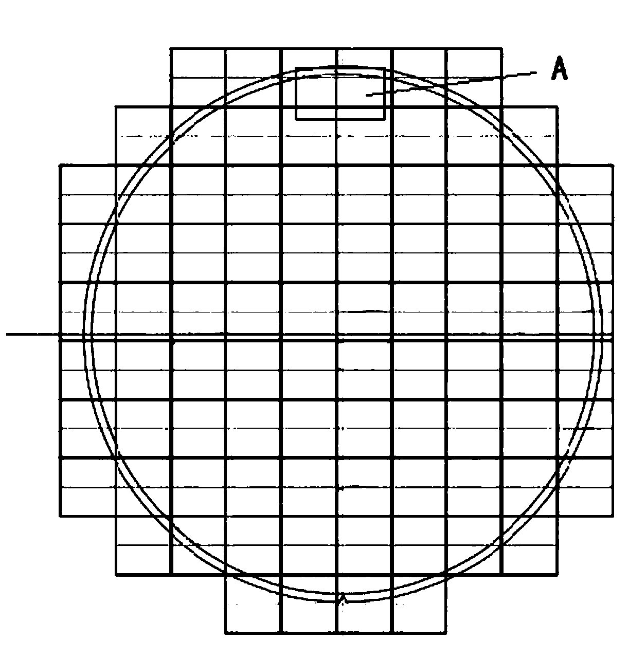
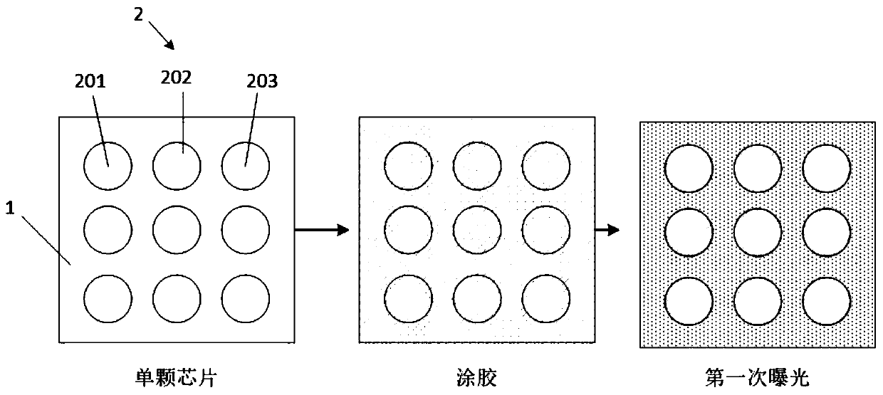
One problem with step-by-step exposure is that it is impossible to modify specific special areas due to the exposure according to the field. According to the normal operation method, the wafer identification code (wafer ID) area will be covered, resulting in the wafer identification code (wafer ID). ) cannot be identified, and with the improvement of chip performance requirements, the number of bumps on a single chip is increasing, and the bump spacing is getting smaller and smaller. When the bump spacing is smaller than the bump diameter, double exposure cannot guarantee the wafer ID area. Completely covered by photoresist and not plated, resulting in the risk of wafer misplacement during subsequent operations, which may cause a series of major problems

Method used


Image

  • Exposure method capable of ensuring identifiability of Wafer ID through multiple times of exposure
  • Exposure method capable of ensuring identifiability of Wafer ID through multiple times of exposure
  • Exposure method capable of ensuring identifiability of Wafer ID through multiple times of exposure

Examples


Embodiment 1

[0043] Due to the requirement of bump height in wafer-level packaging, only stepwise exposure can be used, but stepwise exposure cannot modify special areas. For example, according to the normal working method, wafer ID ) The area will be covered, which will cause the wafer ID to be unrecognized. This will cause the wafer ID to be unrecognized in the subsequent operations and the wafer position will be deviated, which will cause larger problems. The existing solution is CN101089730A patent By double exposure and adjusting the amount of exposure to avoid unnecessary exposure on the edge of the chip in the non-wafer ID area connected to the wafer ID area, and negative photoresist residues are formed, thereby solving the problem of solder bump position information, but as the chip is integrated With higher requirements, the number of bumps will increase, which will cause the spacing between the bumps to become smaller and smaller, so that it is difficult to solve the problem of waf...


PUM


Abstract

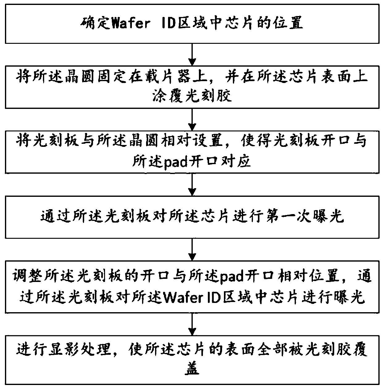
The invention discloses an exposure method capable of ensuring identifiability of a Wafer ID through multiple times of exposure The exposure method comprises the following steps of determining the position of a chip in a wafer ID region; fixing the wafer on a wafer carrier, and coating a photoresist on the surface of the chip; enabling a photoetching plate and the wafer to be arranged oppositely,so that the opening of the photoetching plate corresponds to the opening of a pad; carrying out exposure on the chip for the first time through the photoetching plate; adjusting the relative positionof the opening of the photoetching plate and the opening of the pad, and carrying out exposure on the chip in the Wafer ID region through the photoetching plate; and carrying out development treatmentto enable the surface of the chip to be completely covered with the photoresist. According to the method, the wafer identification code region can be completely covered by the photoresist through multiple times of translational exposure, so that the correct identification of the wafer identification code is ensured, and a series of significant problems caused by the fact that the wafer position is misplaced in the subsequent process are avoided.

Description

Technical field [0001] The present invention relates to the field of semiconductor technology, and in particular to an exposure method that guarantees the recognizability of the Wafer ID through multiple exposures. Background technique [0002] Wafer Level Packaging (WLCSP) adopts the wafer operation mode in the integrated circuit chip manufacturing plant, that is, the entire wafer is packaged and then cut to obtain a large number of finished chips at one time. Compared with traditional packaging, it has the advantages of high packaging efficiency, light, thin, short, and small chip size, high I / O density, and good electrical connection performance after packaging. It is the development trend of advanced packaging. For wafer-level packaging, there are two commonly used exposure methods: proximity exposure and contact exposure. Proximity exposure uses stepper exposure, that is, exposure is performed according to the area (field), and the exposure window size is equal to the field...

Claims


Application Information

Patent Timeline
IPC IPC(8): G03F7/20H01L21/027
CPCG03F7/2022H01L21/0274
Inventor 方梁洪李春阳任超罗立辉彭祎刘明明
Owner NINGBO CHIPEX SEMICON
Learn More