Amplifier circuit and output drive circuit thereof

A technology for outputting drive circuits and amplifier circuits, applied in the direction of output power conversion devices, DC power input conversion to DC power output, instruments, etc., can solve the problems of high production cost, large circuit area, large transistor size, etc., and achieve reduction Production cost and the effect of reducing the circuit area

Inactive Publication Date: 2019-10-11
MEDIATEK SINGAPORE PTE LTD SINGAPORE
View PDF4 Cites 3 Cited by
  • Summary
  • Abstract
  • Description
  • Claims
  • Application Information

AI Technical Summary

Problems solved by technology

When the cross-voltage across the transistor M1 or M2 is higher than 1.8 volts, the transistor M1 or M2 will be easily damaged, and the life cycle of the transistor M1 and M2 will be shortened, thus resulting in a problem of reduced reliability of the amplifier circuit.
Moreover, when the load resistance R_load is small (for example, the load resistance R_load is 37.5 ohm) and the voltage swing of the output voltage is large, the output current Iout can be between 21.5 mA and 64 mA. In order to withstand such a large current, the transistor needs to have a larger size, which will occupy a larger circuit area, resulting in the problem of high production cost

Method used


Image

  • Amplifier circuit and output drive circuit thereof
  • Amplifier circuit and output drive circuit thereof
  • Amplifier circuit and output drive circuit thereof

Examples


Embodiment Construction

[0016] In order to make the above and other objects, features and advantages of the present invention more comprehensible, preferred embodiments are listed below and described in detail with accompanying drawings.

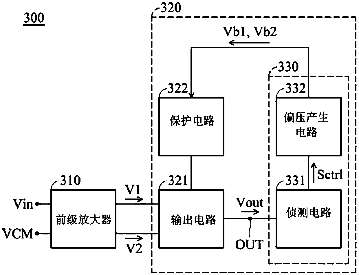
[0017] image 3 A block diagram of an amplifier circuit according to an embodiment of the present invention is shown. According to an embodiment of the present invention, the amplifier circuit 300 may include a pre-amplifier 310 and an output driver circuit 320 . The pre-amplifier 310 is coupled to a predetermined voltage source and a signal input terminal IN for receiving a predetermined voltage VCM and an input voltage Vin, and outputs a first amplified signal V1 and a second amplified signal V2. The output driving circuit 320 is coupled to the pre-amplifier 310 for receiving the first amplified signal V1 and the second amplified signal V2 (also can be regarded as the first input signal and the second input signal of the output driving circuit 320), and drives ...


PUM


Abstract

The invention provides an amplifier circuit and an output drive circuit thereof. The output drive circuit is used for receiving and driving a first input signal and a second input signal and comprisesan output circuit, a protection circuit and a bias control circuit. The output circuit is used for generating an output voltage at the signal output end according to the first input signal and the second input signal. The protection circuit is coupled to the output circuit and used for adjusting the voltage across two terminals of at least one electronic component of the output circuit accordingto the first bias voltage and the second bias voltage, so that the voltage across the two terminals is smaller than a predetermined voltage value. The bias control circuit is coupled to the signal output terminal, and is used for detecting the voltage level of the output voltage and dynamically adjusting the first bias voltage and the second bias voltage according to the voltage level of the output voltage.

Description

technical field [0001] The present invention relates to an amplifier circuit and its output driving circuit, in particular to an amplifier circuit suitable for various circuits with small load resistance, large output signal swing and driving large current. Background technique [0002] Generally speaking, a communication system (eg, a digital television system, a mobile communication system, etc.) transmits a signal to a receiving device through a communication medium. In many communication systems, the receiving device is often located far from the transmitting device, in which case signal loss can occur. Therefore, communication systems generally use amplifiers in transmitting and / or receiving devices to increase the voltage level of signals. [0003] figure 1 A circuit diagram of an amplifier is shown. The amplifier circuit 100 is an operational amplifier receiving a predetermined voltage VCM and an input voltage Vin for generating an output voltage Vout according to ...

Claims


Application Information

Patent Timeline
Patent Type & Authority Applications(China)
IPC IPC(8): H02M3/158
CPCH02M3/158
Inventor 张洋施明
Owner MEDIATEK SINGAPORE PTE LTD SINGAPORE
Why Eureka
Try Eureka