
Array-type multi-makeup PCB splitting method

A PCB board, array technology, applied in the field of array multi-imposition PCB sub-board, can solve the problems of multi-process cost, easy to scratch other products and electronic components, no competitive advantage, etc., to achieve neat board edges and no residues Effect

Inactive Publication Date: 2019-10-11
GUANGDONG KINGSHINE ELECTRONICS TECH CO LTD
View PDF4 Cites 5 Cited by
  • Summary
  • Abstract
  • Description
  • Claims
  • Application Information

AI Technical Summary

Problems solved by technology

[0003] After the stamp hole connection type board is divided, there are residual boards, which are easy to scratch other products and electronic components, and a part left on the edge of the board will also affect the assembly efficiency
[0004] The design of the connection block requires a professional splitter to split the board, and it is necessary to purchase special equipment and molds. For industries with fierce competition, one more process costs more, and there is no competitive advantage

Method used


Image

  • Array-type multi-makeup PCB splitting method

Examples


Embodiment Construction

[0016] The technical solutions in the embodiments of the present invention will be clearly and completely described below in conjunction with specific embodiments. A kind of array type multi-imposition PCB splitting method that is convenient for splitting, comprises the following steps:

[0017] (1) Remove the design of the stamp hole and the connecting block, and reduce the single spacing to 0.4mm;

[0018] (2) Pre-process: including material cutting, drilling, copper sinking, board electrical, dry film and graphic electrical, then etching, AOI, solder mask, and finally engraving text;

[0019] (3) CNC: carry out data design and export data, drill positioning holes after arranging the milling cutters, punch pins, put on the board, start the CNC equipment to remove the PCB sub-board frame, and finally collect the PCB sub-board;

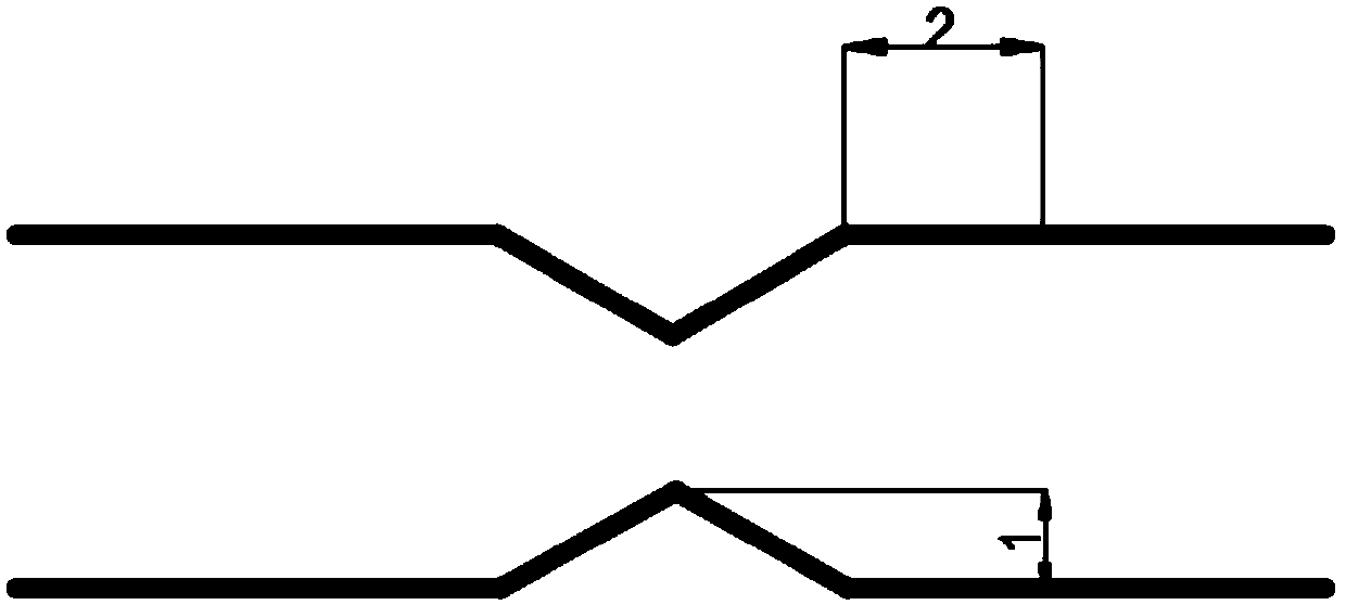
[0020] (4) Use a V-CUT knife to open corresponding V-shaped grooves on both sides of the designed PCB sub-board, the depth of the V-shaped groove is...


PUM


Abstract

The invention relates to the technical field of PCB splitting methods, and particularly discloses an array-type multi-makeup PCB splitting method. The method comprises the following steps: (1) removing stamp holes and connecting blocks, and reducing the distance between PCBs to 0.4 mm; (2) executing a pre-process; (3) performing CNC; (4) forming V-shaped grooves in the two faces of a designed PCBsub-board through a V-CUT knife, wherein the depth of the V-shaped grooves is 1 / 3 of the thickness of the whole PCB, and the angle of the V-CUT knife is 30 degrees; (5) performing a subsequent process, and then reserving safety belts (0.1 mm) at two sides of the V-shaped grooves to prevent the circuit from being damaged during board splitting. Compared with the prior art, the method has the advantages that residual boards after board splitting are reduced, other circuit boards are prevented from being scratched, the assembly efficiency is improved, the distance is reduced, and the board utilization rate is also improved, so that the method can reduce the PCB material cost while guaranteeing the customer quality requirements and reducing the customer cost.

Description

technical field [0001] The invention relates to the technical field of PCB splitting, and specifically discloses an array type multi-imposition PCB splitting method. Background technique [0002] PCB is the mother of electronic products. It carries various electronic components and plays the role of interconnection and conduction of electrical appliances. In order to improve the installation efficiency of components, electronics factories usually adopt multi-piece array imposition design, and the design between impositions Usually there are stamp hole connection type and 2-4mm connection block connection type. [0003] After the stamp hole connection type board is divided, there are residual boards, which are easy to scratch other products and electronic components, and the remaining part on the edge of the board will also affect the assembly efficiency. [0004] The design of the connection block requires a professional splitter to split the board, and it is necessary to p...

Claims


Application Information

Patent Timeline
IPC IPC(8): H05K3/00
CPCH05K3/0052
Inventor 郑晓蓉曾祥福周刚
Owner GUANGDONG KINGSHINE ELECTRONICS TECH CO LTD
Learn More