Display panel, display device and display panel processing method
A display panel and processing method technology, which is applied to semiconductor devices, electrical components, circuits, etc., can solve problems such as short life of blue light-emitting units, and achieve the effect of improving life
- Summary
- Abstract
- Description
- Claims
- Application Information
AI Technical Summary
Problems solved by technology
Method used
Image


Examples
Embodiment Construction
[0048] The specific embodiments of the present invention will be described in detail below in conjunction with the accompanying drawings. It should be understood that the specific embodiments described here are only used to illustrate and explain the present invention, and the present invention is not limited to the following specific embodiments.
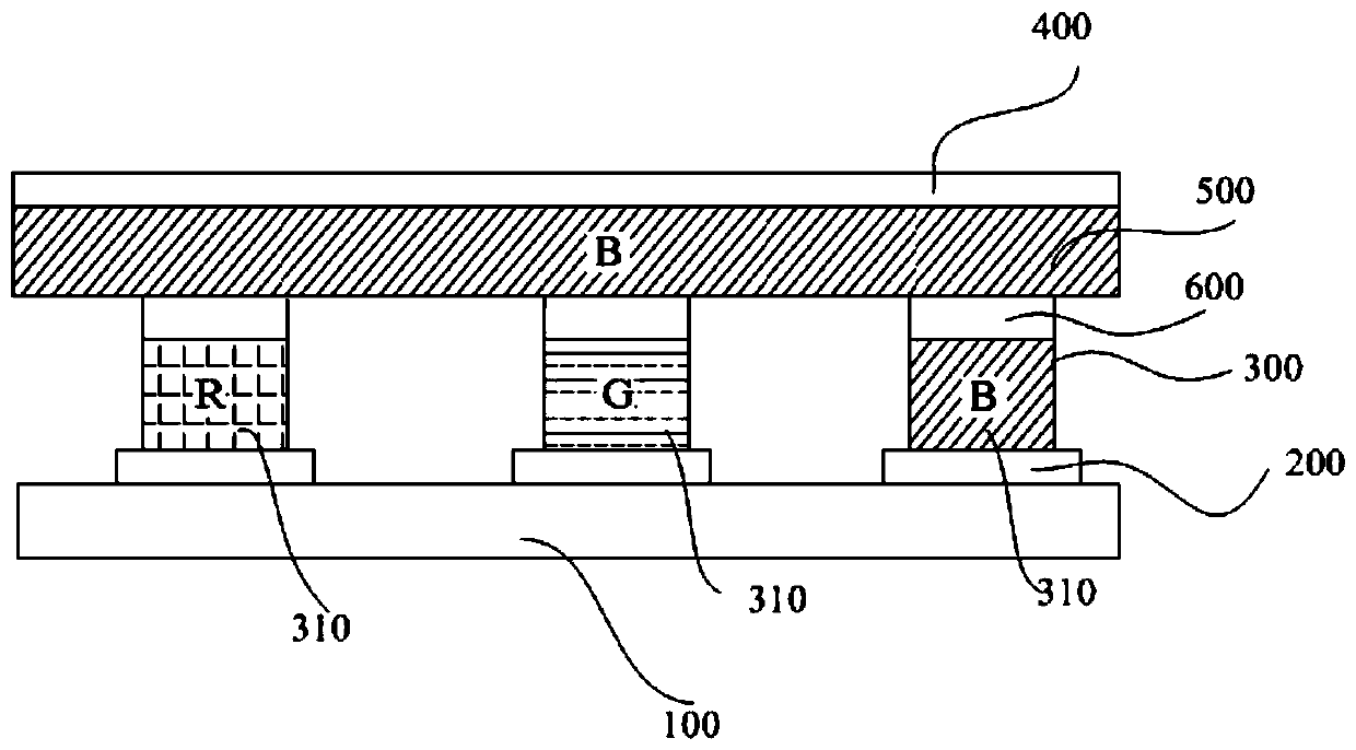
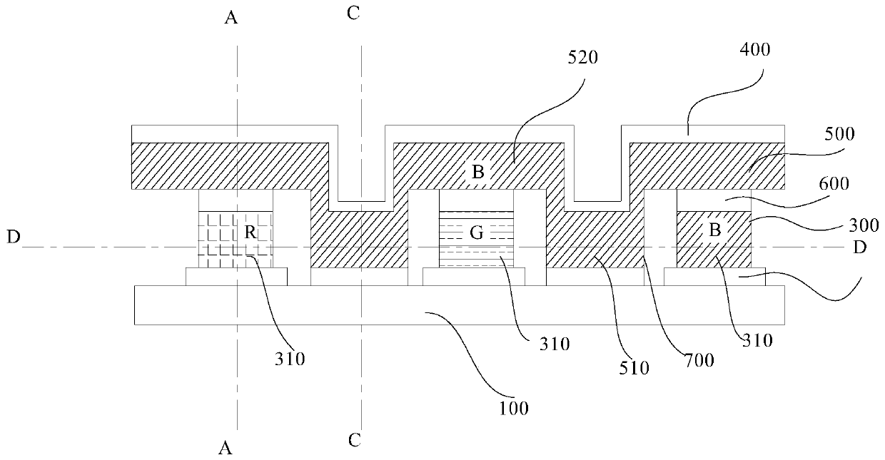
[0049] figure 1 It is a schematic structural diagram of Embodiment 1 of the display panel of the present invention. In the figure, R, G, and B respectively represent the colors of the light emitted by the light-emitting unit or the sub-light-emitting layer, and R is red, G is green, and B is blue. Please refer to figure 1 , the present embodiment provides a display panel including: a substrate 100 and a first electrode layer 200 , a light emitting layer 300 , and a second electrode layer 400 sequentially stacked on the substrate 100 ; the light emitting layer 300 includes a plurality of Light-emitting area, each light-emitting ar...
PUM
 Abstract
Description
Claims
Application Information
 - R&D
- Intellectual Property
- Life Sciences
- Materials
- Tech Scout
- Unparalleled Data Quality
- Higher Quality Content
- 60% Fewer Hallucinations
Browse by: Latest US Patents, China's latest patents, Technical Efficacy Thesaurus, Application Domain, Technology Topic, Popular Technical Reports.
© 2025 PatSnap. All rights reserved.Legal|Privacy policy|Modern Slavery Act Transparency Statement|Sitemap|About US| Contact US: help@patsnap.com