High-precision PCB plate separating device

A high-precision, sub-board technology, used in metal processing, electrical components, insulation substrate/layer processing, etc. Powder, reasonable structure design, high work efficiency

Pending Publication Date: 2019-10-25
广东中孚智能装备有限公司
View PDF0 Cites 2 Cited by
  • Summary
  • Abstract
  • Description
  • Claims
  • Application Information

AI Technical Summary

Problems solved by technology

With the further development of science and technology, people's demand for PCB is getting higher and higher. The existing PCB splitting mechanism currently has low cutting accuracy, and has high cutting loss rate, complicated installation, difficult maintenance and high cost. , slow response speed, can not realize the shortcomings of automatic continuous operation, therefore, needs further improvement

Method used


Image

  • High-precision PCB plate separating device
  • High-precision PCB plate separating device
  • High-precision PCB plate separating device

Examples


Embodiment Construction

[0025] The implementation of the present invention will be described in detail below in conjunction with the accompanying drawings. The accompanying drawings are only for reference and description, and do not constitute a limitation to the protection scope of the present invention.

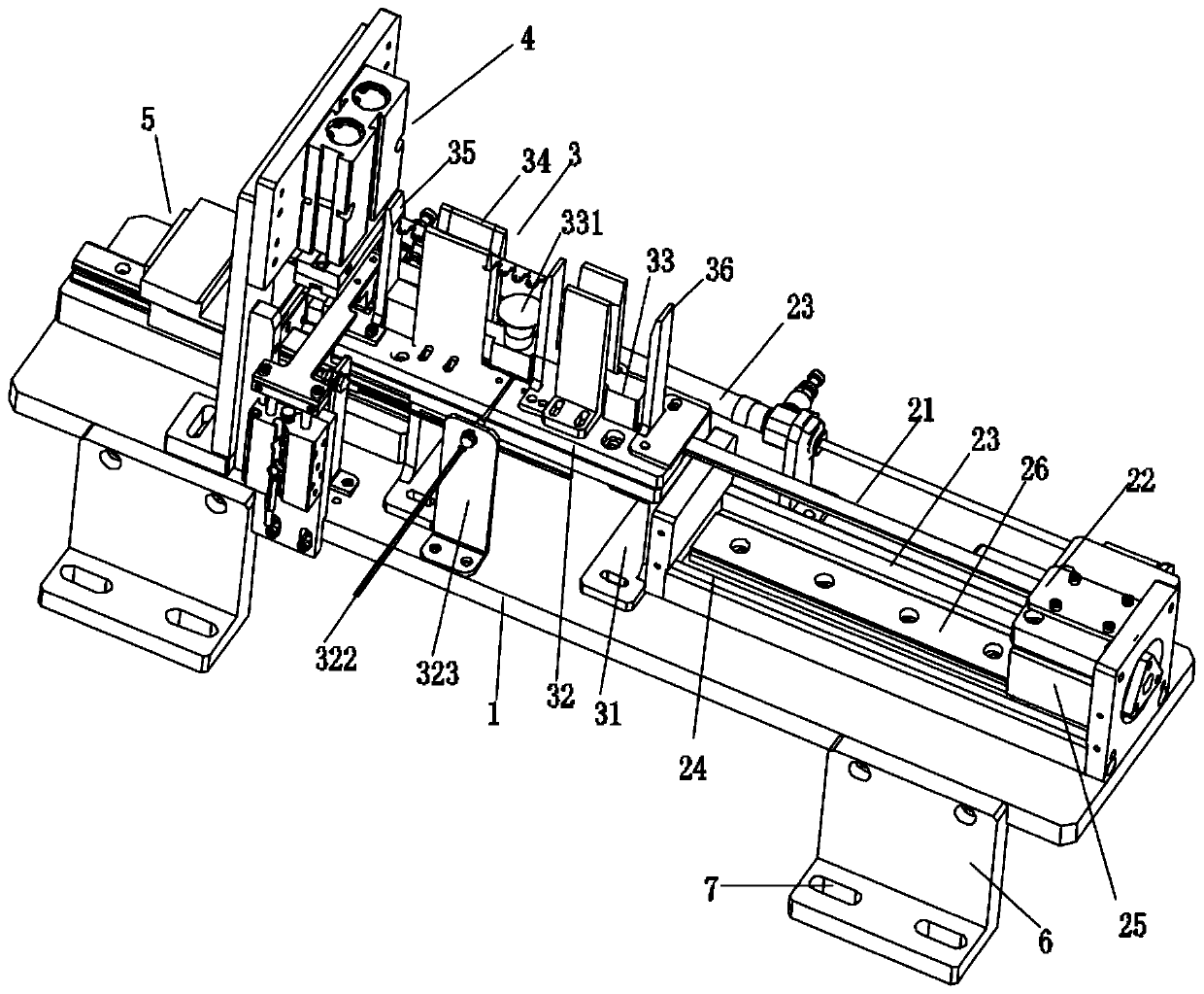
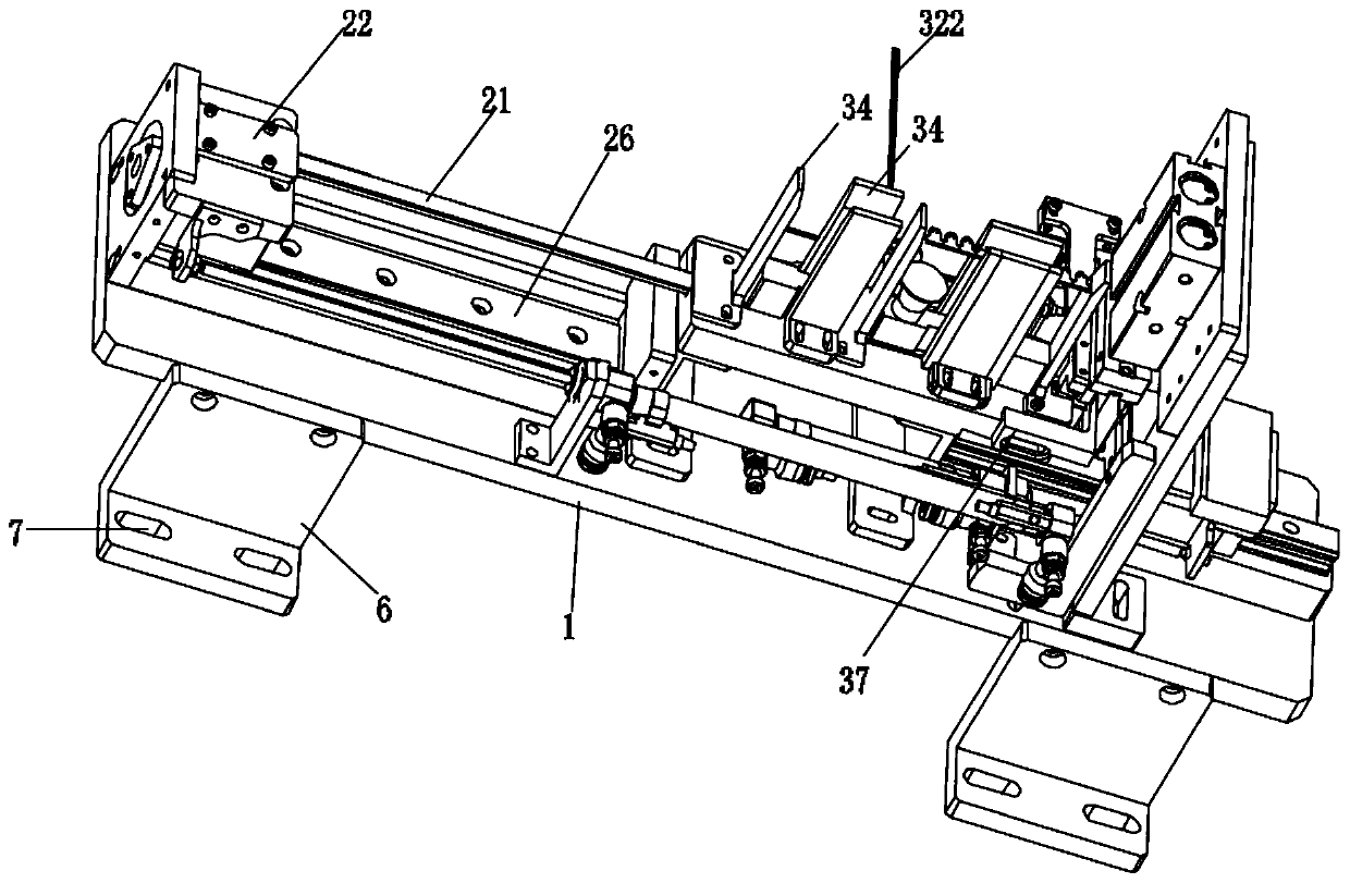
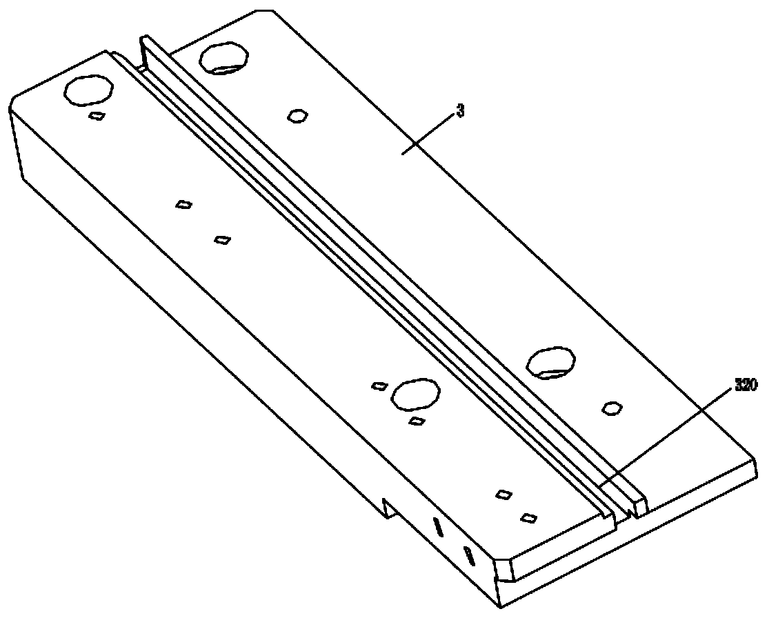
[0026] Such as Figure 1-8 As shown, the present invention provides a high-precision PCB splitting device, including a main frame 1, and the main frame 1 is provided with a pushing structure 2, a pressing structure 3, a material cutting structure 4, and a loading structure 5. The pushing structure 2 is connected with the pressing structure 3, the pressing structure 3 is connected with the cutting structure 4, the loading structure 5 is arranged on one side of the cutting structure 4, and the pressing structure 3 Used to fix PCB materials, the pusher structure 2 is used to push the PCB materials in the pressing structure 3 to the cutting structure 4, the loading structure 5 is used to collect the c...


PUM


Abstract

The invention provides a high-precision PCB plate separating device. The device comprises a main machine frame, wherein the main machine frame is sequentially provided with a pushing structure, a material pressing structure, a material cutting structure and a material loading structure, the material pushing structure and the material pressing structure are connected, and the material pressing structure is connected with the material cutting structure. One side of the material cutting structure is provided with the material loading structure, the material pressing structure is used for fixing PCB materials, the material pushing structure is used for pushing the PCB materials of the material pressing structure to the material cutting structure, and the material loading structure used for collecting cut materials. The main machine frame is provided with a support block, wherein the support block is provided with fixing adjusting through holes. The high-precision PCB plate separating device has the advantages of being reasonable in structural design, high in working efficiency, easy to maintain and convenient to use.

Description

technical field [0001] The invention relates to the technical field of PCB processing, in particular to a high-precision PCB splitting device. Background technique [0002] PCB is an important electronic component, a support for electronic components, and a carrier for electrical connections of electronic components. Because it is made by electronic printing, it is called "printed" circuit board. As the support of electronic components, PCB is the carrier of electrical connection of electronic components. PCBs are widely used as components of electrical devices in various industries. PCB has played a huge role in various industries. With the further development of science and technology, people's demand for PCB is getting higher and higher. The existing PCB splitting mechanism currently has low cutting accuracy, and has high cutting loss rate, complicated installation, difficult maintenance and high cost. , slow response, can not realize the shortcomings of automatic conti...

Claims


Application Information

Patent Timeline
IPC IPC(8): B26D1/08B26D7/06B26D7/02B26D7/32H05K3/00
CPCB26D1/085B26D7/0608B26D7/025B26D7/32H05K3/0052B26D2007/322
Inventor 李浩亮邵春霞王毅
Owner 广东中孚智能装备有限公司
Why Eureka
Try Eureka