Display panel, display device and method for manufacturing display panel

A technology for display panels and graphics, applied in semiconductor/solid-state device manufacturing, semiconductor devices, electrical components, etc., can solve the problems of uneven thickness of pixel units, poor film uniformity, etc., to speed up the spreading speed, reduce the concentration difference, improve the The effect of film uniformity

Active Publication Date: 2021-07-20
KUNSHAN GO VISIONOX OPTO ELECTRONICS CO LTD
View PDF12 Cites 0 Cited by
  • Summary
  • Abstract
  • Description
  • Claims
  • Application Information

AI Technical Summary

Problems solved by technology

[0004] In view of this, embodiments of the present invention provide a display panel, a display device, and a method for manufacturing a display panel to solve the problems of uneven thickness of pixel units and poor uniformity of film layers in existing display panels.

Method used


Image

  • Display panel, display device and method for manufacturing display panel
  • Display panel, display device and method for manufacturing display panel
  • Display panel, display device and method for manufacturing display panel

Examples


Embodiment Construction

[0030] The following will clearly and completely describe the technical solutions in the embodiments of the present invention with reference to the accompanying drawings in the embodiments of the present invention. Obviously, the described embodiments are only some of the embodiments of the present invention, not all of them. Based on the embodiments of the present invention, all other embodiments obtained by persons of ordinary skill in the art without making creative efforts belong to the protection scope of the present invention.

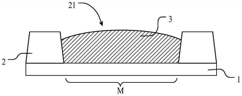
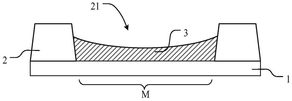
[0031] Figure 1a Shown is a schematic diagram of a first state of preparing a pixel unit of a conventional display panel. Figure 1b Shown is a schematic diagram of the second state of preparing the pixel unit of the conventional display panel. specifically, Figure 1a Shown is a schematic diagram of the state of the pixel unit 3 before drying, Figure 1b Shown is a schematic diagram of the state of the pixel unit 3 after drying. Such as Figu...


PUM


Abstract

Embodiments of the present invention refer to a display panel, a display device, and a method for manufacturing a display panel, which solve the problems of uneven thickness of pixel units and poor film layer uniformity of pixel units in existing display panels. The display panel includes a pixel defining layer and a conductive layer laminated with the pixel defining layer, a first surface of the conductive layer is provided with a wetting pattern, wherein the first surface is a surface adjacent to the pixel defining layer. In the display panel provided by the embodiment of the present invention, by setting the wetting pattern on the first surface adjacent to the conductive layer and the pixel defining layer, the spreading speed of the ink droplets is accelerated, the concentration difference of the ink droplets is reduced, and the final improvement is achieved. The uniformity of the film layer of the pixel unit is ensured, and the luminous performance of the display device is guaranteed.

Description

technical field [0001] The invention relates to the field of display technology, in particular to a display panel, a display device and a method for preparing a display panel. Background technique [0002] Organic light-emitting diode (Organic Light-Emitting Diode, OLED) display devices occupy an important position in the field of display technology due to their many advantages such as thinness, high brightness, low power consumption, and high definition. At present, in the preparation process of OLED display devices, pixel units of OLED display devices are usually prepared based on inkjet printing technology. Specifically, an inkjet printing process is used to inject ink material into the pixel container to form ink droplets, and the ink droplets spread in the pixel container to finally form pixel units. [0003] However, during the spreading process of the ink droplet, the solvent volatilization rate is different between the edge area and the central area of ​​the ink dro...

Claims


Application Information

Patent Timeline
Patent Type & Authority Patents(China)
IPC IPC(8): H01L27/32H01L51/56
CPCH10K71/135H10K59/122H10K71/00
Inventor 邱岳毛祖攀
Owner KUNSHAN GO VISIONOX OPTO ELECTRONICS CO LTD
Why Eureka
Try Eureka