Electrostatic capacitance detection device

a capacitance detection and electrostatic technology, applied in the direction of resistance/reactance/impedence, instruments, acquiring/reconforming fingerprints/palmprints, etc., can solve the problems of insufficient protective measures, dielectric layer breakage, and peripheral circuit breakage, etc., to improve durability, simple structure, and increase the thickness of the capacitance detection dielectric layer

Active Publication Date: 2007-04-24
138 EAST LCD ADVANCEMENTS LTD
View PDF16 Cites 26 Cited by
  • Summary
  • Abstract
  • Description
  • Claims
  • Application Information

AI Technical Summary

Benefits of technology

[0010]An advantage of the invention is to provide an electrostatic capacitance detection device that can assuredly protect a circuit from an instantaneous current with a simple structure without occurring any breakages, etc.
[0011]An electrostatic capacitance detection device that reads surface contours of a target object by detecting an electrostatic capacitance, which changes according to a distance from the target object, according to an aspect of the invention includes an electrostatic capacitance detection element arranged in a matrix of M rows and N columns, and a power supply line that supplies a power source to the electrostatic capacitance detection element. The electrostatic capacitance detection element includes a signal detection element storing a charge corresponding to the electrostatic capacitance and a signal amplification element amplifying a signal corresponding to the charge stored by the signal detection element. The signal detection element includes a capacitance detection electrode and a capacitance detection dielectric layer disposed on a side that the target object comes in contact with of the capacitance detection electrode. Particularly, the capacitance detection dielectric layer includes an insulator and a semiconductor layer.
[0012]According to the configuration, upon approaching of the target object such as fingerprint, etc., to the electrostatic capacitance detection element, a voltage corresponding to whether the target object is contacted or not is produced in the capacitance detection electrode. The voltage is amplified by the signal amplification element so that electrostatic capacitance detection is conducted corresponding to whether ridges in a fingerprint, etc are contacted or not. Since the dielectric constant of the semiconductor layer is larger than that of the insulator, the thickness of the capacitance detection dielectric layer can be increased, improving durability. Here, in a case where the target object is charged, if the charge is not released via a path, an instantaneous current flows from the capacitance detection electrode to a peripheral circuit upon approaching of the target object, causing a circuit breakdown due to an electrostatic discharge. On this point, according to the configuration, the charge of the target object does not flow directly via the capacitance detection electrode since the insulator is provided to the capacitance detection dielectric layer. In addition, according to the configuration, since the semiconductor layer is provided, an inversion layer is formed on the surface of the semiconductor layer just before the target object contacts the semiconductor layer, so that charges of the target object quickly spreads over the surface of the semiconductor layer. As a result, circuits can be prevented from a breakdown due to the electrostatic discharge.
[0013]Here, it is preferable that the semiconductor layer is disposed on the uppermost surface of the electrostatic capacitance detection element. This configuration allows the inversion layer to be formed in the semiconductor layer before the target object is contacted, so that the charge is released. Moreover, even if the target object contacts the capacitance detection dielectric layer, the instantaneous current does not flow directly to the circuit since the insulator is further formed between the semiconductor layer and the capacitance detection electrode. As a result, the circuit can be prevented from the breakdown due to the electrostatic discharge.
[0014]Here, an electrical resistance RPP of the semiconductor layer is represented by the following equation:
[0015]RPP>10·ΔτCAEquation⁢⁢1where Δτ is measurement time of the electrostatic capacitance detection element, and CA is a target object electrostatic capacitance.

Problems solved by technology

When the target object having a charge, it often causes a breakdown of a peripheral circuit due to an instantaneous current induced by a discharge.
As above-mentioned, since the thickness of the dielectric layer cannot be increased, the dielectric layer is often broken due to worn off by rubbing with fingers, etc.
As a result, it is not enough for protective measures.
Once a part of the components for discharge is broken, the instantaneous current flows directly into the wiring and peripheral circuits, resulting in the breakdown of the peripheral circuits.
Here, in a case where the target object is charged, if the charge is not released via a path, an instantaneous current flows from the capacitance detection electrode to a peripheral circuit upon approaching of the target object, causing a circuit breakdown due to an electrostatic discharge.

Method used


Image

  • Electrostatic capacitance detection device
  • Electrostatic capacitance detection device
  • Electrostatic capacitance detection device

Examples


example 1

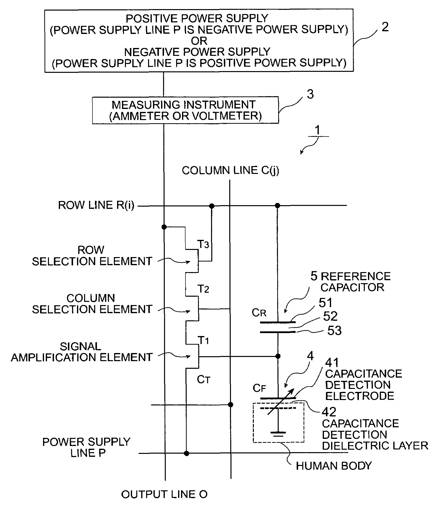
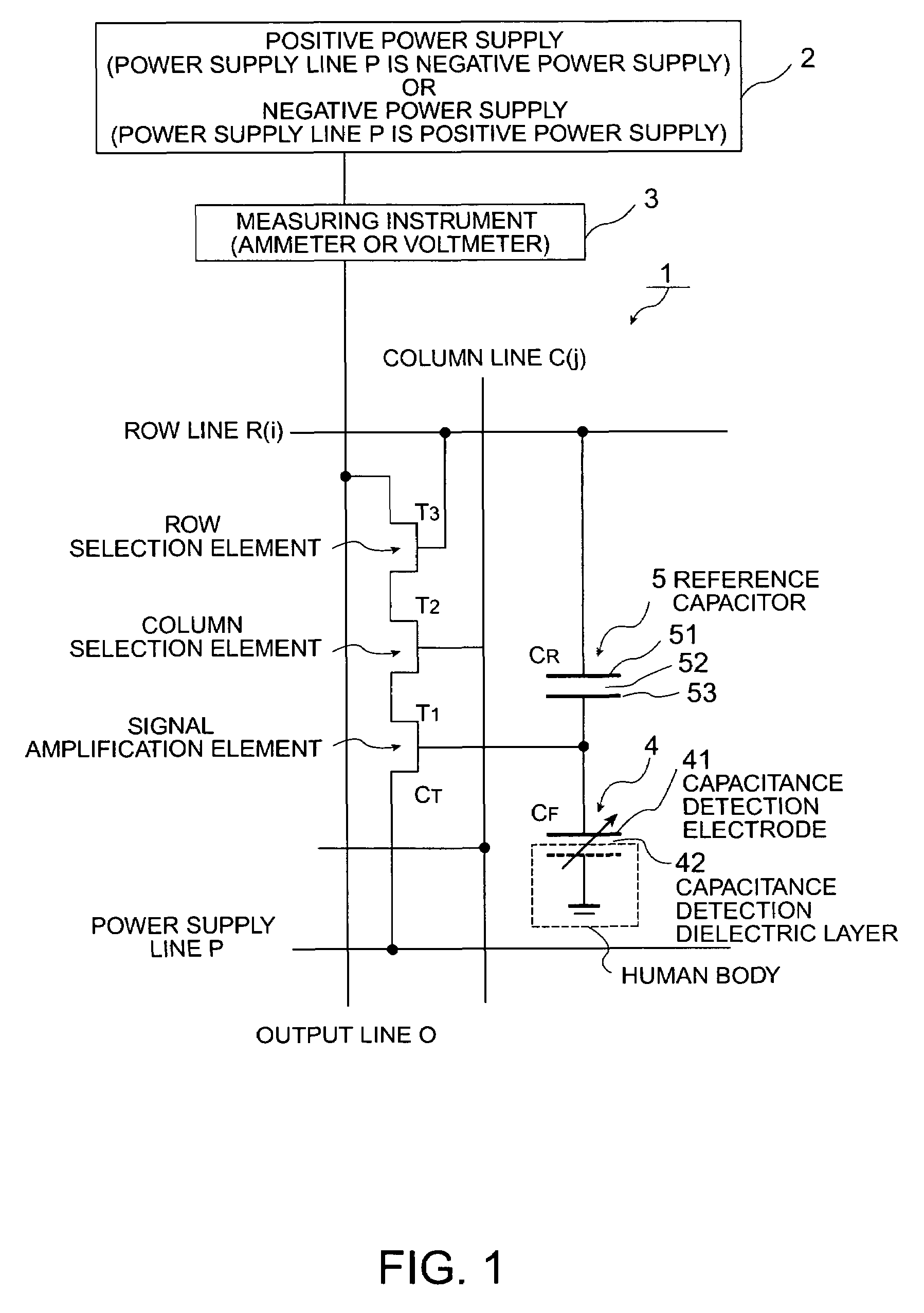
[0122]An electrostatic capacitance detection device made up of thin film semiconductor devices was fabricated on a glass substrate. The fabricated electrostatic capacitance detection device was then transferred to a plastic substrate using known transfer technology. The circuit configuration is the same as that in the embodiment. The electrostatic capacitance detection device includes electrostatic capacitance detection elements arranged in a matrix of 304 rows and 304 columns. The array is a square, 20 mm on a side.

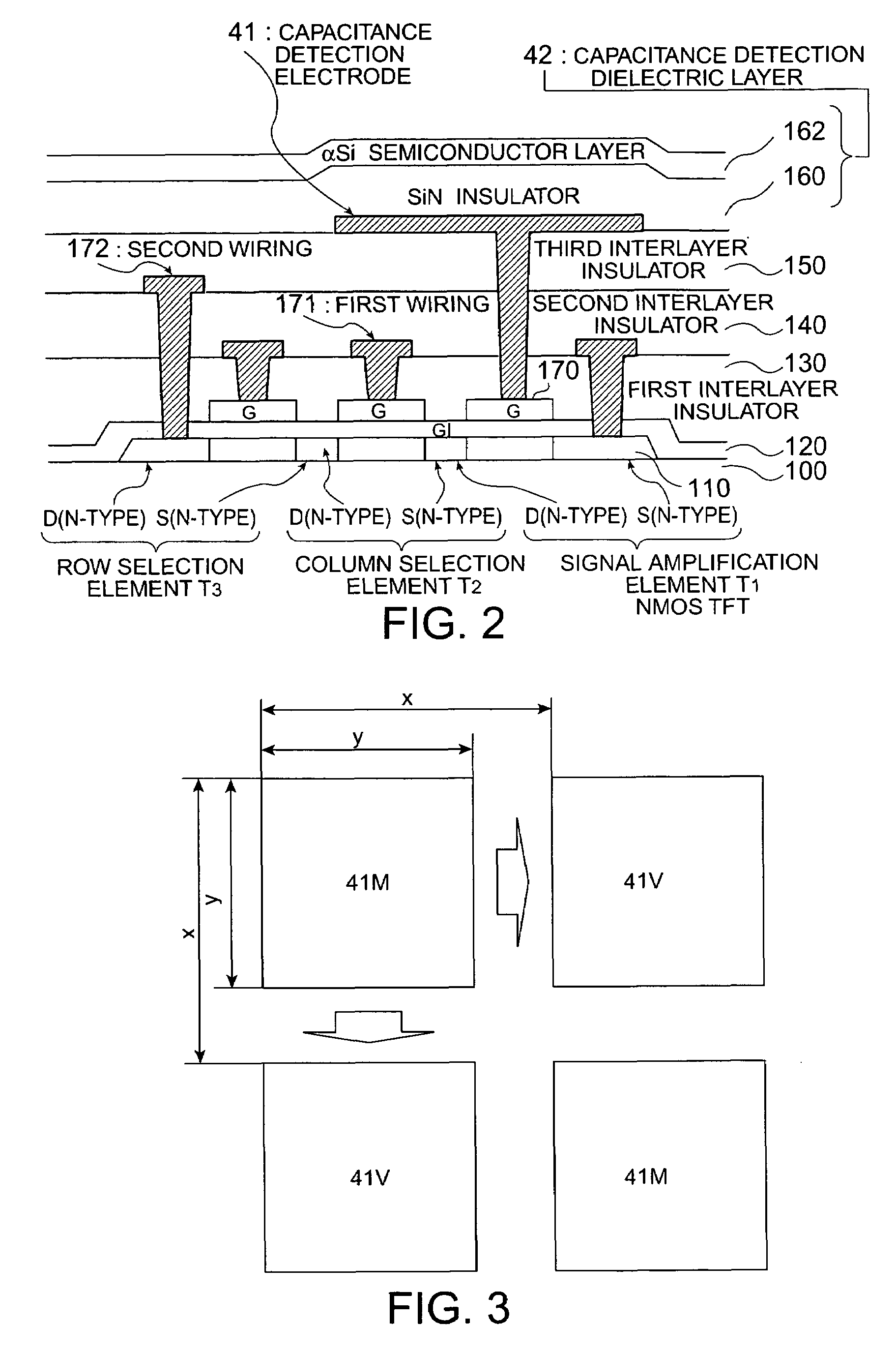
[0123]Below, details will be described by corresponding to the layer structure shown in FIG. 2. The substrate 100, made of poly-ether-sulfone (PES), has a thickness of 200 μm. The signal amplification element T1, the column selection element T2, and the row selection element T3 are all fabricated with N-type thin film semiconductor devices. The thin film semiconductor devices are a top-gate type, as shown in FIG. 2. They are fabricated in a low-temperature process where ...


PUM


Abstract

An electrostatic capacitance detection device includes an electrostatic capacitance detection element arranged in M rows and N columns. The electrostatic capacitance detection element includes a signal detection element that retains a charge in proportion to the electrostatic capacitance. The signal detection element includes a capacitance detection electrode and a capacitance detection dielectric layer formed on the capacitance detection electrode. The capacitance detection dielectric layer includes a first semiconductor layer and an insulator disposed between the capacitance detection electrode and the first semiconductor layer. A signal amplification element amplifies a signal corresponding to the retained charge in the signal detection element. The signal amplification element includes a second semiconductor layer different from the first semiconductor layer. A power supply line supplies a power source to the electrostatic capacitance detection element.

Description

RELATED APPLICATION INFORMATION[0001]This application claims priority to Japanese Patent Application No. 2004-298019, filed Oct. 12, 2004, whose contents are expressly incorporated herein by reference.BACKGROUND OF THE INVENTION[0002]1. Technical Field[0003]The present invention relates to an electrostatic capacitance detection device that reads the surface contours of a fingerprint or other target object having extremely small ridges and valleys by detecting electrostatic capacitance, which changes according to the distance from the surface of the target object.[0004]2. Related Art[0005]Conventionally, electrostatic capacitance detection devices used for fingerprint sensors, etc., are fabricated so that a sensor electrode and a protective film such as a dielectric provided on the sensor electrode are formed on a substrate as described in examples of related art listed as follows: Japanese Unexamined Patent Publication No. 2000-346610 is a first example of related art; Japanese Unex...

Claims


Application Information

Patent Timeline
Patent Type & Authority Patents(United States)
IPC IPC(8): G01R27/26
CPCG06K9/0002G01R27/26G06V40/1306G06F18/00
Inventor MIYASAKA, MITSUTOSHI
Owner 138 EAST LCD ADVANCEMENTS LTD
Why Eureka
Try Eureka