
Array substrate and display panel

A technology for array substrates and display areas, applied to semiconductor devices, electrical components, circuits, etc., can solve the problems of large delay of data signal waveforms, different resistances, uneven brightness of signal line pixels, etc., and achieve the effect of reducing resistance and reducing impedance differences

Active Publication Date: 2019-11-05
EVERDISPLAY OPTRONICS (SHANGHAI) CO LTD
View PDF4 Cites 8 Cited by
  • Summary
  • Abstract
  • Description
  • Claims
  • Application Information

AI Technical Summary

Problems solved by technology

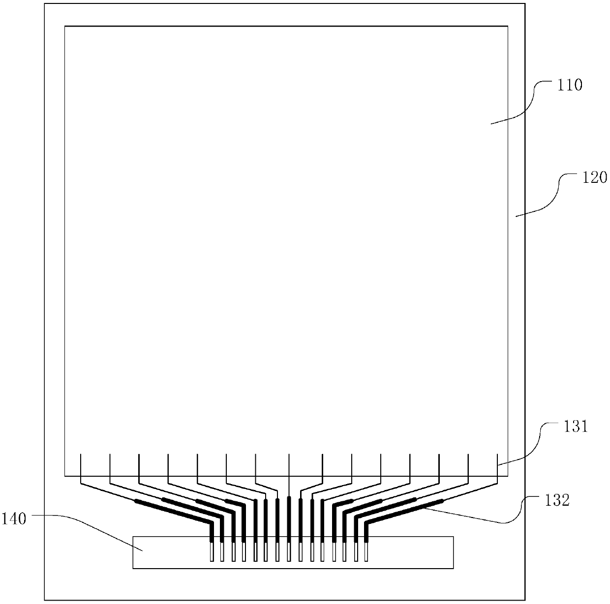
[0005] Different signal lines have different resistances due to different lengths. Therefore, when the signal is loaded, the waveform delay of the data signal transmitted on the different signal lines is too large, which makes the pixel brightness controlled by the signal line uneven. , affecting the display effect

Method used


Image

  • Array substrate and display panel
  • Array substrate and display panel
  • Array substrate and display panel

Examples


Embodiment Construction

[0024] Example embodiments will now be described more fully with reference to the accompanying drawings. Example embodiments may, however, be embodied in many forms and should not be construed as limited to the embodiments set forth herein; rather, these embodiments are provided so that this disclosure will be thorough and complete, and will fully convey the concept of example embodiments to those skilled in the art. The same reference numerals denote the same or similar structures in the drawings, and thus their repeated descriptions will be omitted.

[0025] The described features, structures, or characteristics may be combined in any suitable manner in one or more embodiments. In the following description, numerous specific details are provided in order to give a thorough understanding of embodiments of the invention. However, those skilled in the art will appreciate that the technical solutions of the present invention may be practiced without one or more of the specific...


PUM


Abstract

The invention provides an array substrate and a display panel. The array substrate comprises a display area and a non-display area. The array substrate comprises a first metal layer, a second metal layer, a drive chip and a third metal layer, wherein a plurality of gate lines are formed inside the display area on the first metal layer and the second metal layer, the first metal layer and / or the second metal layer extend / extends to the non-display area from the display area, and a plurality of first signal connecting lines are formed inside the non-display area; the drive chip is positioned inside the non-display area; a plurality of data lines are formed inside the display area on the third metal layer, a plurality of second signal connecting lines are formed on the third metal layer, eachsecond signal connecting line is led out from the drive chip, and each second signal connecting line is electrically connected with one corresponding first signal connecting line extending to the non-display area from the display area respectively so as to form a signal transmission line, the electrical resistivity of the third meta layer is smaller than that of the first metal layer and that ofthe second metal layer, and the difference value of impedance among the signal transmission lines is smaller than a preset threshold value. According to the array substrate and the display panel provided by the invention, the display effect is improved.

Description

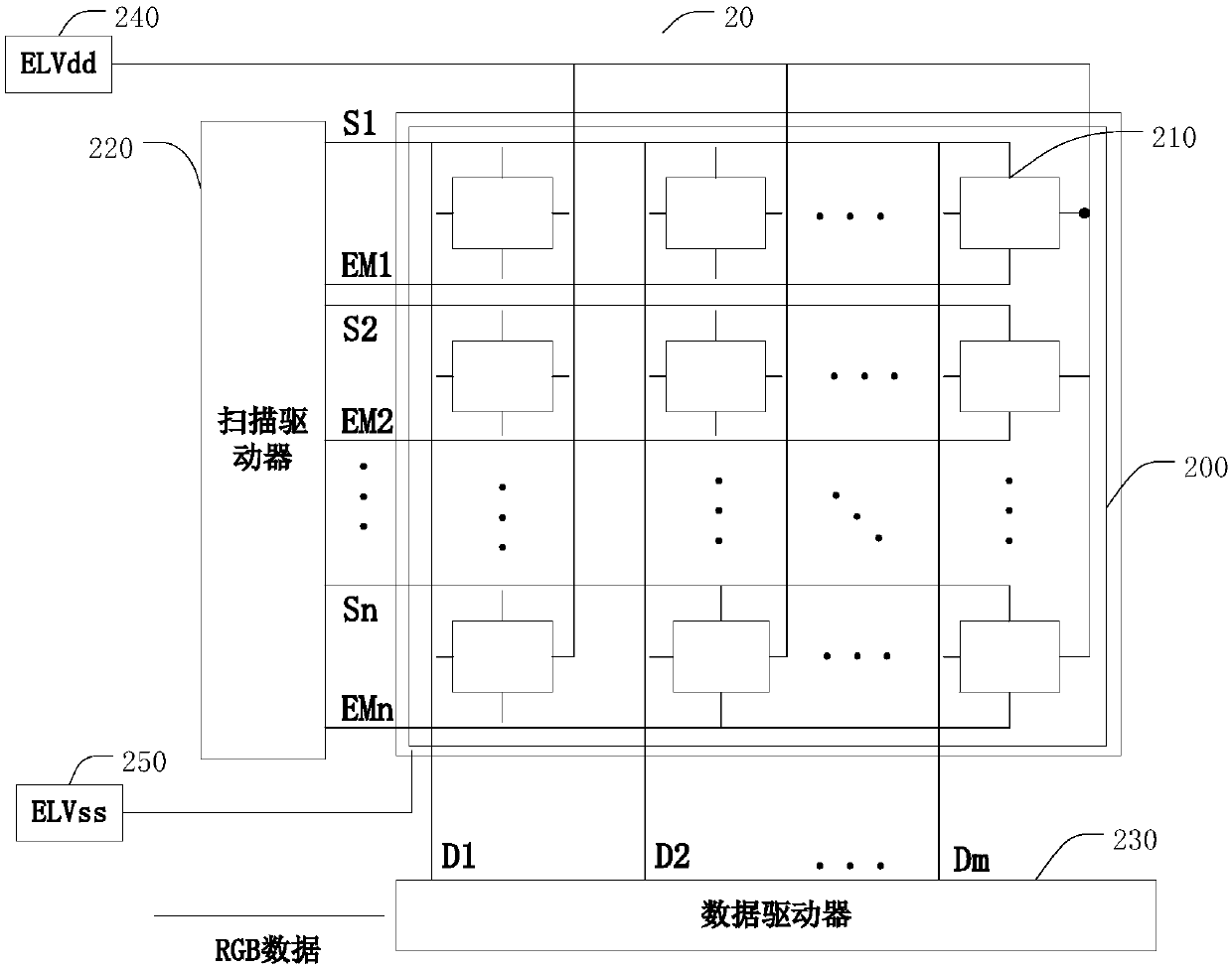
technical field [0001] The present invention relates to the field of display technology, in particular to an array substrate and a display panel. Background technique [0002] In recent years, OLED (Organic Light-Emitting Diode, Organic Light-Emitting Diode) technology has developed rapidly, and has become a promising technology most likely to replace LCD (Liquid Crystal Display, Liquid Crystal Display). [0003] In the prior art, after the data lines or gate lines of the display panel are concentrated in the non-display area, they are introduced into several specific pad areas arranged on the periphery of the display panel to realize signal transmission with the driver chip [0004] Since the signal lines such as data lines or gate lines are different from the pad area, for example, in the area where the signal lines are concentrated, the signal lines near the edge of the display panel are the longest and have the largest resistance, while the signal lines located in the ce...

Claims


Application Information

Patent Timeline
Patent Type & Authority Applications(China)
IPC IPC(8): H01L27/32
CPCH10K59/1315
Inventor 周思思
Owner EVERDISPLAY OPTRONICS (SHANGHAI) CO LTD
Learn More