
Display panel and display device

A display panel and display area technology, applied in the direction of electrical components, electric solid devices, circuits, etc., can solve problems such as film peeling, achieve the effect of increasing the contact area and avoiding film peeling

Inactive Publication Date: 2019-11-12
WUHAN CHINA STAR OPTOELECTRONICS SEMICON DISPLAY TECH CO LTD
View PDF5 Cites 5 Cited by
  • Summary
  • Abstract
  • Description
  • Claims
  • Application Information

AI Technical Summary

Problems solved by technology

[0004] The invention provides a display panel and a display device to alleviate the technical problem of film layer peeling in the existing display panel

Method used


Image

  • Display panel and display device
  • Display panel and display device
  • Display panel and display device

Examples


Embodiment Construction

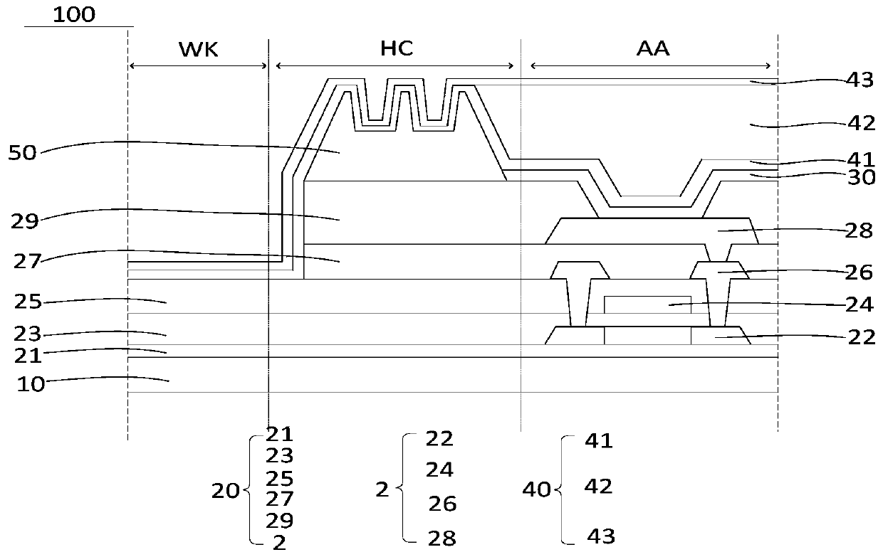
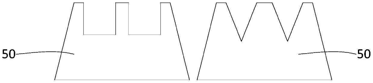
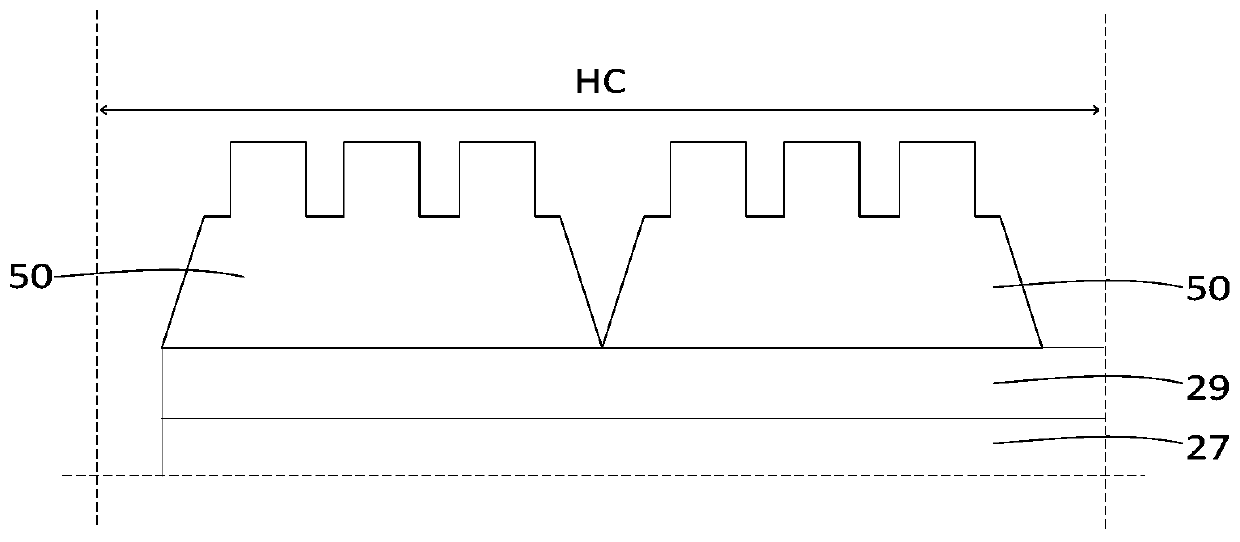
[0031] The following descriptions of the various embodiments refer to the accompanying drawings to illustrate specific embodiments in which the invention may be practiced. The directional terms mentioned in the present invention, such as [top], [bottom], [front], [back], [left], [right], [inside], [outside], [side], etc., are only for reference The orientation of the attached schema. Therefore, the directional terms used are used to illustrate and understand the present invention, but not to limit the present invention. In the figures, structurally similar elements are denoted by the same reference numerals.

[0032] The embodiment of the present invention can alleviate the technical problem of film layer peeling in the existing display panel.

[0033] In one embodiment, as figure 1 As shown, a display panel 100 is provided, including a display area AA, a hole-digging area WK, and a buffer zone HC between the display area AA and the hole-digging WK ​​area; the display panel...


PUM


Abstract

The invention provides a display panel and a display device. The display panel includes a display area, a hole digging area, and a buffer area between the display area and the hole digging area. One or more retaining walls are formed on a pixel defining layer in the buffer area, and the top surface of the retaining wall is provided with at least one groove or protrusion; a packaging layer is arranged on a light-emitting functional layer and the retaining wall, and the contact area between the top surface of the retaining wall and the packaging layer is greater than the projection area of the positive projection of the top surface of the retaining wall on the substrate. Through arranging the groove or the protrusion on the top surface of the retaining wall in the buffer area, the contact area between the top surface of the retaining wall and the packaging layer is increased, and the problem of film layer peeling between the retaining wall and the packaging layer is avoided.

Description

technical field [0001] The present invention relates to the field of display technology, in particular to a display panel and a display device. Background technique [0002] There is a new type of O-cut OLED display panel, which is characterized in that an O-shaped through hole is designed in its non-edge display area, and modules such as cameras, infrared sensors, and earpieces can be placed under the O-shaped through hole. Since the position of this O-shaped through hole can be set arbitrarily, it can realize the flexibility of the position of the under-screen camera, infrared sensor, earpiece and other modules in the panel display area. Currently, in order to ensure the flexibility of OLED panels, TFE (Thin Film Encapsulation) technology is usually used for encapsulation and protection. TFE usually includes inorganic, organic, and inorganic laminated structures. The inorganic layer is usually deposited by chemical vapor deposition (CVD), physical vapor deposition (PVD) o...

Claims


Application Information

Patent Timeline
Patent Type & Authority Applications(China)
IPC IPC(8): H01L27/32H01L51/52
CPCH10K59/122H10K59/873H10K50/844H10K71/00H10K59/1201
Inventor 孙佳佳
Owner WUHAN CHINA STAR OPTOELECTRONICS SEMICON DISPLAY TECH CO LTD
Learn More