
Heat dissipation mainboard and optical module

A technology for motherboards and heat sinks, applied in the field of optical communications, can solve problems such as poor heat dissipation of chips, achieve convenient assembly, solve heat dissipation difficulties, and reduce heat transfer thermal resistance

Pending Publication Date: 2019-11-15
DONGGUAN MENTECH OPTICAL & MAGNETIC
View PDF0 Cites 8 Cited by
  • Summary
  • Abstract
  • Description
  • Claims
  • Application Information

AI Technical Summary

Problems solved by technology

[0004] The purpose of this application is to provide a heat dissipation motherboard and an optical module to solve the technical problem of poor heat dissipation of the chip when the chip is packaged on the PCB board using the COB process in the prior art

Method used


Image

  • Heat dissipation mainboard and optical module
  • Heat dissipation mainboard and optical module
  • Heat dissipation mainboard and optical module

Examples


Embodiment Construction

[0029] The technical solutions of the present invention will be clearly and completely described below in conjunction with the accompanying drawings. Apparently, the described embodiments are some of the embodiments of the present invention, but not all of them.

[0030] The components of the embodiments of the invention generally described and shown in the figures herein may be arranged and designed in a variety of different configurations. Accordingly, the following detailed description of the embodiments of the invention provided in the accompanying drawings is not intended to limit the scope of the claimed invention, but merely represents selected embodiments of the invention.

[0031] Based on the embodiments of the present invention, all other embodiments obtained by persons of ordinary skill in the art without making creative efforts belong to the protection scope of the present invention.

[0032] In the description of the present invention, it should be noted that the...


PUM

PropertyMeasurementUnit
Thermal conductivityaaaaaaaaaa

Abstract

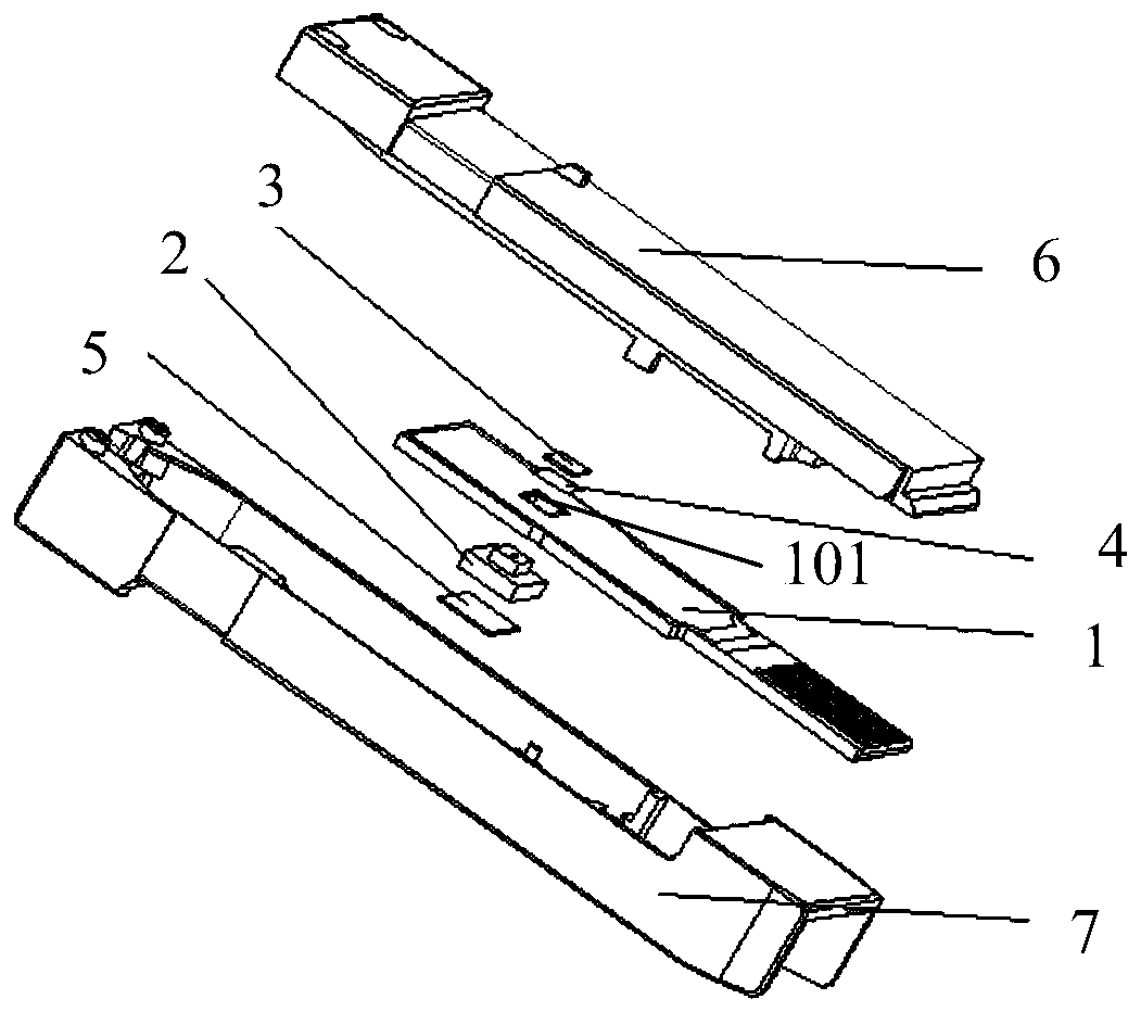
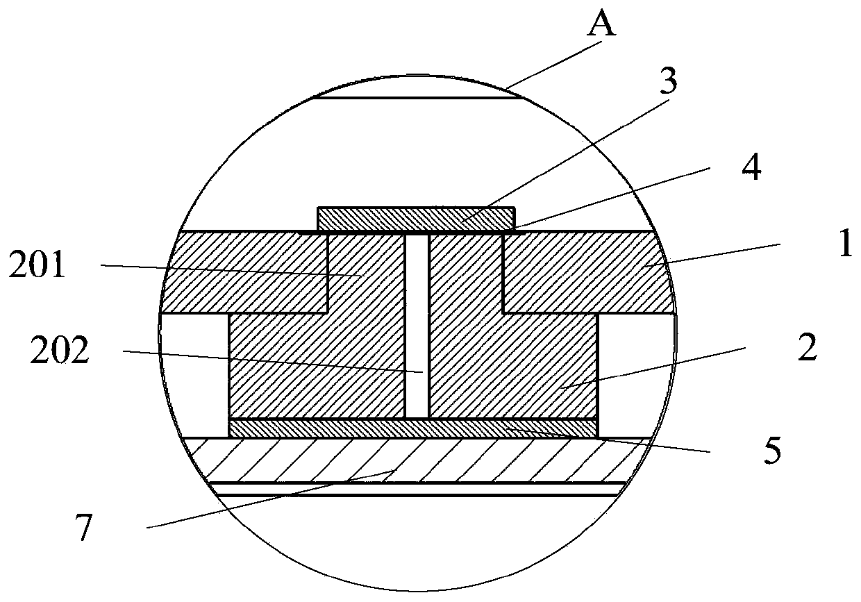
The invention relates to the technical field of optical communication, in particular to a heat dissipation mainboard and an optical module. The heat dissipation mainboard is used for packaging a chipand comprises a circuit board and a heat dissipation piece. The heat dissipation piece is located on one side of the circuit board. The chip is arranged on the other side of the circuit board. A heatdissipation through hole is formed at a position, corresponding to the chip, of the circuit board and penetrate through the two sides of the circuit board. At least one part of the heat dissipation piece extends into the heat dissipation through hole and can make contact with the chip, so that heat generated when the chip works can be transmitted out, heat transfer resistance is reduced. The effective heat dissipation is achieved on the chip. The problem that a COB bare chip is difficult to dissipate heat is solved. The optical module comprises the heat dissipation mainboard, a chip and a shell. The heat dissipation mainboard and the chip are located in the shell. The heat dissipation piece of the heat dissipation mainboard makes contact with the chip and the shell respectively so that heat generated by the chip can be rapidly transmitted to the shell. Therefore, the effect of efficient heat dissipation is achieved.

Description

technical field [0001] The invention relates to the technical field of optical communication, in particular to a heat dissipation main board and an optical module. Background technique [0002] In the field of optical communication, it is often necessary to use the COB (chip on board) process to package chips with specific functions on the PCB (printed circuit board), and the current mainstream method is to paste the chip on a specific chip on the PCB. area. However, after the chip is attached to the PCB, the heat cannot be directly transferred to the corresponding metal shell by using a thermal interface material or a metal heat dissipation block, which makes this process have a large heat dissipation disadvantage. [0003] In response to the above problems, the current conventional practice is to drill through holes in the COB area of ​​the PCB and use overheating holes for heat dissipation. However, due to the limited content of the thermally conductive material at the ...

Claims


Application Information

Patent Timeline
IPC IPC(8): H01L23/367H01L23/373H01L23/467H05K1/02
CPCH01L23/367H01L23/3735H01L23/3736H01L23/467H05K1/0206
Inventor 张家学吴春付李珍周军王艳红
Owner DONGGUAN MENTECH OPTICAL & MAGNETIC
Learn More