Micro-light-emitting diode display panel, preparation method of micro-light-emitting diode display panel, spliced display panel and device

A technology of micro-light-emitting diodes and display panels, which is applied in the direction of identification devices, instruments, electrical components, etc., can solve the problems that affect the production yield of products, difficult to control the chamfer size, and difficult to realize the process, so as to improve the production yield, The effect of reducing size and reducing process difficulty

Pending Publication Date: 2019-11-26
BOE TECH GRP CO LTD
View PDF9 Cites 27 Cited by
  • Summary
  • Abstract
  • Description
  • Claims
  • Application Information

AI Technical Summary

Problems solved by technology

However, the current narrow frame is basically difficult to achieve a narrow frame on all sides, especially for micro & mini LED display products, it is necessary to use splicing technology to achieve large-size display
In the existing technology, circuits are formed on the upper and lower sides of the micro & mini LED display panel, and then the front and back circuits are electrically connected through the side wiring scheme of the silver paste, so that the bonding (Bonding) area can be canceled to achieve a borderless design, but the side Lead wire technology requires chamfering on the glass edge, and due to the brittleness of glass, chamfering on the glass edge in the existing technology is prone to chamfering and chipping, and because the chamfer size is difficult to control, the process is more difficult to realize
[0003] To sum up, the narrow bezel technology of micro & mini LED display panels in the existing technology is difficult to process, and chamfering and edge chipping are prone to lead wire damage, which affects product production yield.

Method used


Image

  • Micro-light-emitting diode display panel, preparation method of micro-light-emitting diode display panel, spliced display panel and device
  • Micro-light-emitting diode display panel, preparation method of micro-light-emitting diode display panel, spliced display panel and device
  • Micro-light-emitting diode display panel, preparation method of micro-light-emitting diode display panel, spliced display panel and device

Examples


Embodiment Construction

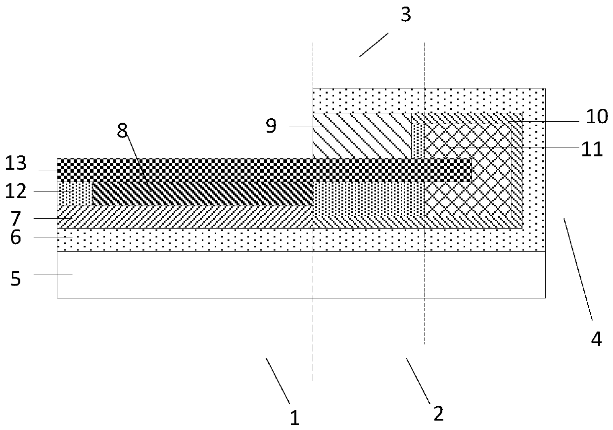
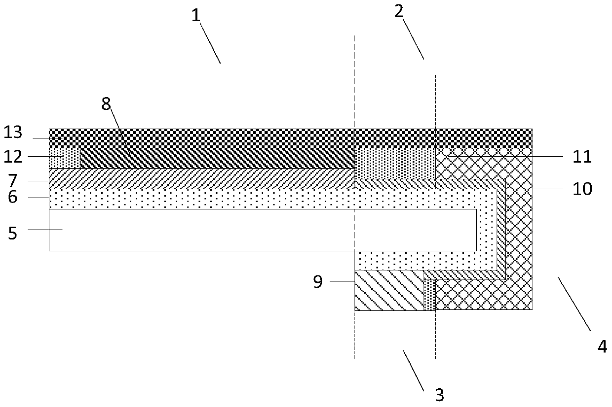
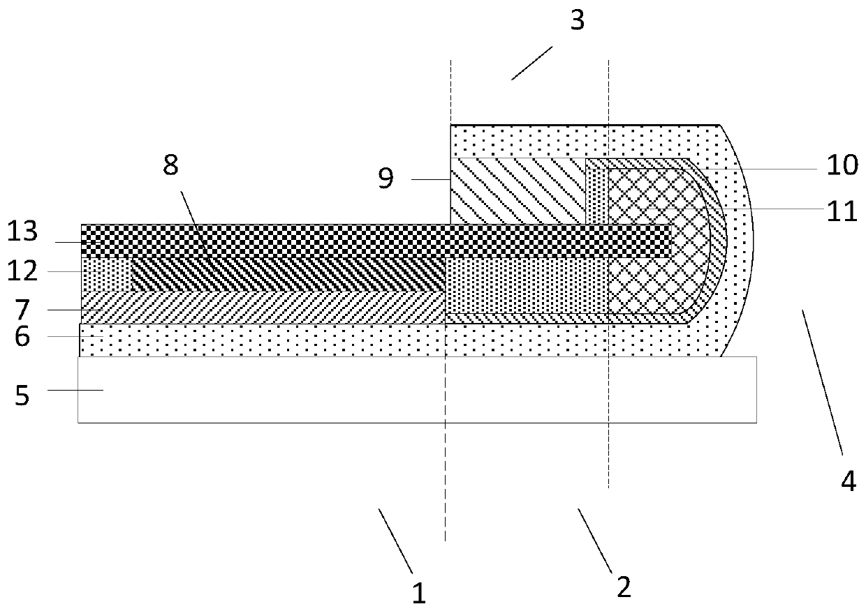
[0060] The embodiment of the present application provides a micro light emitting diode display panel, such as figure 1 As shown, the micro light emitting diode display panel is divided into: a display area 1 and a peripheral area 2 outside the display area 1; the peripheral area 2 includes: a fan-out area 3, and a peripheral area located in the fan-out area 3 and the bending area 4 between the display area 1;

[0061] The display area 1 includes: a base substrate 5, a flexible buffer layer 6 on the base substrate, a pixel circuit 7 on the flexible buffer layer 6, and a pixel circuit 7 on the pixel circuit 7. micro light emitting diode device 8;

[0062] The flexible buffer layer 6 extends to the peripheral area 2;

[0063] The fan-out area 3 further includes: a driving circuit 9 located on the flexible buffer layer 6;

[0064] The bending area 4 also includes: a lead 10 on the flexible buffer layer 6 electrically connecting the pixel circuit 7 and the driving circuit 9, and...


PUM


Abstract

The invention discloses a micro-light-emitting diode display panel, a preparation method of the micro-light-emitting diode display panel, a spliced display panel and a device, and is used for realizing a narrow frame while the yield of the micro-light-emitting diode display panel is ensured. The micro-light-emitting diode display panel provided by the embodiment of the invention is divided into adisplay area and a peripheral area located outside the display area; the peripheral area comprises a fan-out area and a bending area located between the fan-out area and the display area; the displayarea comprises a substrate, a flexible buffer layer, a pixel circuit and a micro-light-emitting diode device, wherein the flexible buffer layer is positioned on the substrate, the pixel circuit is located on the flexible buffer layer, and the micro-light-emitting diode device is located on the pixel circuit; the flexible buffer layer extends to the peripheral area; the fan-out area further comprises a driving circuit located on the flexible buffer layer; the bending area further comprises a lead located on the flexible buffer layer and electrically connected with the pixel circuit and the driving circuit, and a bending protective layer located on the lead; and the bending area is bent along a bending axis.

Description

technical field [0001] The present application relates to the field of display technology, in particular to a micro-light-emitting diode display panel, a preparation method, a spliced ​​display panel, and a device. Background technique [0002] At present, display devices are developing towards ultra-thin, ultra-narrow bezel or even bezel-less. However, the current narrow bezels are basically difficult to achieve narrow four-sided bezels, especially for micro & mini LED display products, which need to use splicing technology to achieve large-size displays. In the existing technology, circuits are formed on the upper and lower sides of the micro & mini LED display panel, and then the front and back circuits are electrically connected through the side wiring scheme of the silver paste, so that the bonding (Bonding) area can be canceled to achieve a borderless design, but the side Lead technology requires chamfering on the glass edge, and due to the brittleness of glass, chamf...

Claims


Application Information

Patent Timeline
Patent Type & Authority Applications(China)
IPC IPC(8): G09F9/33H01L27/15
CPCG09F9/33H01L27/156
Inventor 刘超崔强伟孙海威董学翟明李沛张功涛
Owner BOE TECH GRP CO LTD
Why Eureka
Try Eureka