Display panel and manufacturing method thereof

A technology of display panel and manufacturing method, which is applied in the direction of final product manufacturing, sustainable manufacturing/processing, semiconductor/solid-state device manufacturing, etc. The effect of high rate and simple production method

Active Publication Date: 2019-11-29
WUHAN CHINA STAR OPTOELECTRONICS SEMICON DISPLAY TECH CO LTD
View PDF5 Cites 5 Cited by
  • Summary
  • Abstract
  • Description
  • Claims
  • Application Information

AI Technical Summary

Problems solved by technology

[0005] The present invention provides a display panel, which can enhance the interfacial bonding force between the flexible substrate and the buffer layer, so as to solve the problem of weak bonding between the material of the flexible substrate and the material of the buffer layer in the existing display panel due to its own performance. Poor technical issues that affect the display

Method used


Image

  • Display panel and manufacturing method thereof
  • Display panel and manufacturing method thereof
  • Display panel and manufacturing method thereof

Examples


Embodiment Construction

[0035] The following descriptions of the various embodiments refer to the accompanying drawings to illustrate specific embodiments in which the invention may be practiced. The directional terms mentioned in the present invention, such as [top], [bottom], [front], [back], [left], [right], [inside], [outside], [side], etc., are only for reference The orientation of the attached schema. Therefore, the directional terms used are used to illustrate and understand the present invention, but not to limit the present invention. In the figures, structurally similar elements are denoted by the same reference numerals.

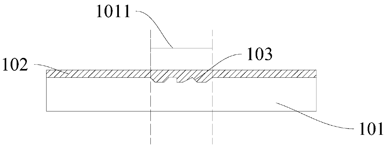
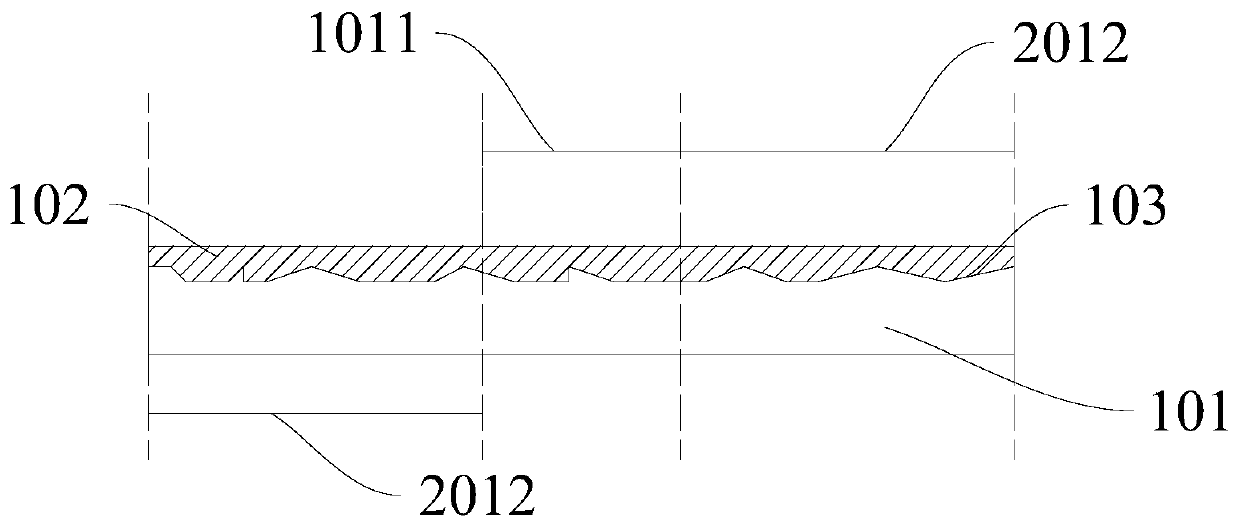
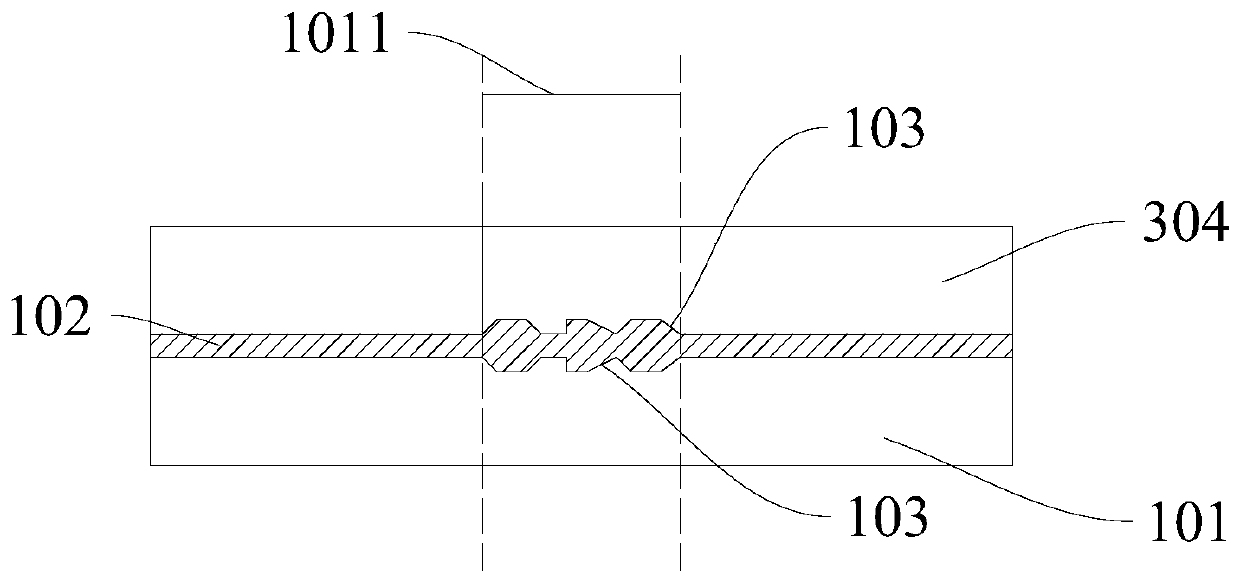
[0036] The present invention aims at the technical problem that the display panel is affected by the poor bonding force between the material of the flexible substrate and the material of the buffer layer due to its own performance in the display panel, and this embodiment can solve this defect.

[0037] see figure 1 , the first embodiment of the present invention prov...


PUM


Abstract

The invention provides a display panel and a manufacturing method thereof. The display panel comprises a bending area. The display panel comprises a first flexible substrate; a buffer layer which is formed on the surface of one side of the first flexible substrate, wherein in the bending area, the surface, in contact with the buffer layer, of the first flexible substrate is of a rough structure. According to the display panel, an interface bonding force between the flexible substrate and the buffer layer can be enhanced, and the problem that the flexible substrate in the bending area is proneto being stripped from the buffer layer can be solved. Meanwhile, the risk that the flexible substrate in the non-bending area is stripped from the buffer layer can be avoided, the display quality isimproved, and the product yield is increased.

Description

technical field [0001] The invention relates to the field of display technology, in particular to a display panel and a manufacturing method thereof. Background technique [0002] At present, most manufacturers use AMOLED (Active-matrix organic light-emitting diode) technology based on flexible polyimide to realize foldable and narrow frame design. Polyimide has better flexibility, so it has the premise of being foldable. By bending the COF (Chip On Film, packaging technology) bonding area of ​​the lower frame or the IC (Integrated Circuit, integrated circuit) bonding area of ​​COP (Chip On Pi, packaging technology) and the lower bending of some traces and circuits, the original The lower frame of the rigid display panel becomes smaller. [0003] However, in the existing display panels, due to the low molecular polarity of polyimide, the bonding force between the polyimide and the buffer layer of silicon dioxide is weak, and the polyimide is prone to peeling off when the d...

Claims


Application Information

Patent Timeline
Patent Type & Authority Applications(China)
IPC IPC(8): H01L51/00H01L27/32
CPCH10K59/12H10K77/111Y02E10/549Y02P70/50H10K59/1201H10K2102/311G02F1/133305H01L33/12G09F9/301H01L33/22H01L33/24G06F1/1641G06F1/1652H10K71/00
Inventor 胡凯
Owner WUHAN CHINA STAR OPTOELECTRONICS SEMICON DISPLAY TECH CO LTD
Why Eureka
Try Eureka