Flexible device transition device and preparation method and flexible device patch method

A flexible device and patch technology, applied in the field of chip packaging, can solve the problems of IC chip damage, difficulty in controlling the accuracy of the patch, and high risks

Active Publication Date: 2019-12-10
INST OF FLEXIBLE ELECTRONICS TECH OF THU ZHEJIANG
View PDF7 Cites 1 Cited by
  • Summary
  • Abstract
  • Description
  • Claims
  • Application Information

AI Technical Summary

Problems solved by technology

[0003] IC chips based on semiconductor materials such as Si, SiC, GaAs are the key components of flexible electronic products. In the current production process of flexible electronic devices, in order to make IC chips have a certain degree of flexibility, thinning process Thinning the substrate of the IC chip, the thinned IC chip is easy to cause damage during the moving process. At the same time, because the IC chip is too thin, too light, and flexible, it is difficult to control the placement accuracy. It will increase the complexity of the subsequent placement process, reduce the product yield and placement efficiency, and is not conducive to the mass production application of flexible IC chips
At the same time, the existing professional equipment for placing ultra-thin IC devices is expensive and the placement efficiency is low
The placement process of flexible IC chips is incompatible with the integrated manufacturing process technology and equipment of electronic products of existing SMT devices, which will result in large investment and high risk in the manufacturing process and equipment of customized development of flexible electronic products

Method used


Image

  • Flexible device transition device and preparation method and flexible device patch method
  • Flexible device transition device and preparation method and flexible device patch method
  • Flexible device transition device and preparation method and flexible device patch method

Examples


Embodiment Construction

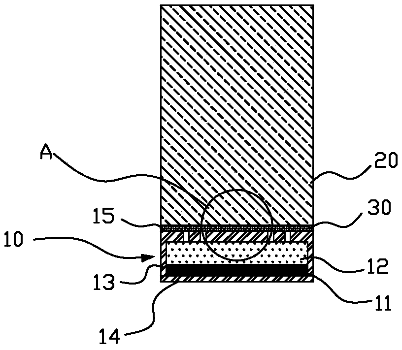
[0075] In order to further explain the technical means and functions adopted by the present invention to achieve the intended invention purpose, the detailed description is as follows in conjunction with the accompanying drawings and preferred embodiments.

[0076] The invention provides a transition device for a flexible device, a method for preparing the transition device, and a method for attaching a flexible device based on the transition device for a flexible device. The transition device for a flexible device can better protect an IC chip, It is convenient for transportation, avoids damage to the IC chip during transportation, and can facilitate the subsequent chip application of the IC chip. The use of the transition device can be directly applied to the manufacture of flexible electronic products.

[0077] The IC chip mentioned in this patent refers to the traditional IC chip with Si, SiC, GaAs and other semiconductor material substrates.

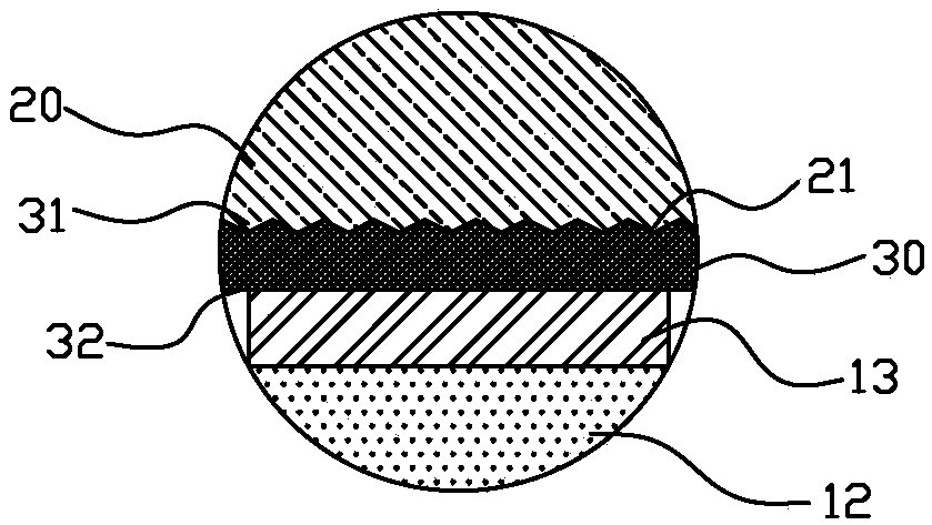
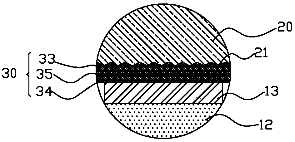
[0078] like figure 1 As sho...


PUM

PropertyMeasurementUnit
thicknessaaaaaaaaaa
thicknessaaaaaaaaaa
thicknessaaaaaaaaaa

Abstract

The invention relates to a flexible device transition device and preparation method and a flexible device patch method. The transition device comprises an IC chip and a transition substrate. The IC chip comprises an IC chip substrate, a circuit function layer formed on the IC chip substrate and a packaging layer. The packaging layer packages the IC chip substrate and the circuit function layer from at least the surface of the circuit functional layer and the side surface of the IC chip. A first surface to be patched with the substrate and a second surface corresponding to the first surface areformed on the IC chip. The transition substrate is adhered to the second surface of the IC chip through an adhesive layer. The flexible device transition device can facilitate back patch applicationof the IC chip and is directly applied to the manufacturing of flexible electronic products. The preparation of the packaging layer greatly protects the IC chip, reduces the requirements on storage conditions and avoids damage to the IC chip during transportation.

Description

technical field [0001] The invention relates to the field of chip packaging, in particular to a transition device for flexible devices, a method for preparing the transition device, and a method for bonding flexible devices based on the transition device for flexible devices. Background technique [0002] In recent years, with the continuous development and progress of flexible electronics technology and the increasingly widespread application of smart wearable products, flexible electronic devices are very popular in the market due to their unique advantages of flexibility, ductility, light weight, and thin thickness. Broad application prospects. [0003] IC chips based on semiconductor materials such as Si, SiC, GaAs are the key components of flexible electronic products. In the current production process of flexible electronic devices, in order to make IC chips have a certain degree of flexibility, thinning process Thinning the substrate of the IC chip, the thinned IC ch...

Claims


Application Information

Patent Timeline
Patent Type & Authority Applications(China)
IPC IPC(8): H01L27/32B81B3/00B81C1/00
CPCB81B3/00B81C1/00134H10K59/88H10K59/00
Inventor 龚云平
Owner INST OF FLEXIBLE ELECTRONICS TECH OF THU ZHEJIANG
Why Eureka
Try Eureka