
Multilayer electronic component and method for manufacturing multilayer electronic component

An electronic component, layered technology, applied in fixed capacitor parts, transformer/inductor parts, electrical components, etc., can solve problems such as stray capacitance, inconvenience, electrode plastic deformation, etc., to suppress defective products, easy-to-create effects

Active Publication Date: 2022-05-17
MURATA MFG CO LTD
View PDF17 Cites 0 Cited by
  • Summary
  • Abstract
  • Description
  • Claims
  • Application Information

AI Technical Summary

Problems solved by technology

[0012] In a multilayer electronic component including a laminated body on which a ceramic layer is laminated, in the same manner as disclosed in Patent Document 1, recesses for displaying symbols, letters, numbers, etc. are formed on the top surface of the laminated body, and in order to suppress noise When the shielding layer is formed on the outer surface of the laminate through penetration, there is a possibility of inconvenience as follows
[0013] First, when a convex portion formed in a mold or the like is to be pressed into the top surface of an unfired laminate to form a concave portion for displaying a mark or the like, the electrode formed directly under the concave portion may be locally pressed to cause plasticity. Deformation may cause the electrode to break and cause cracks in the electrode
In addition, when it is intended to form a concave portion displaying a mark or the like by irradiating laser light on the top surface of the laminated body, there is heat caused by applying laser irradiation to the electrode formed directly under the concave portion, and the electrode is disconnected, and the electrode is disconnected. concern about cracks
[0014] In addition, stray capacitance may occur between the shield layer formed on the inner bottom surface of the concave portion formed on the top surface of the laminate and the electrodes formed inside the laminate, and the desired electrical characteristics may not be obtained.

Method used


Image

  • Multilayer electronic component and method for manufacturing multilayer electronic component
  • Multilayer electronic component and method for manufacturing multilayer electronic component
  • Multilayer electronic component and method for manufacturing multilayer electronic component

Examples


no. 1 Embodiment approach

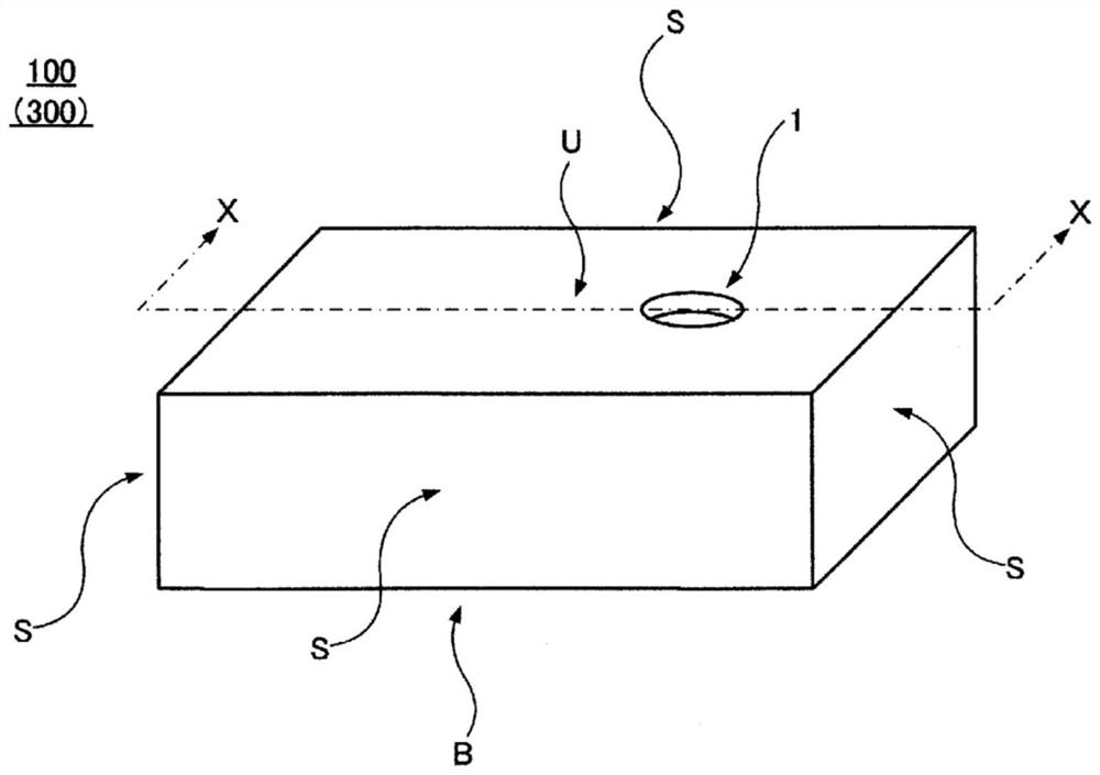
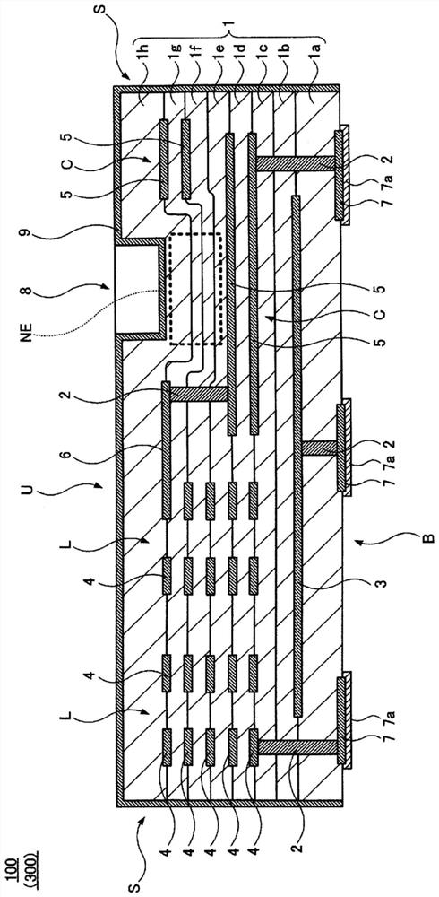
[0040] exist figure 1 , figure 2 The multilayer electronic component 100 according to the first embodiment is shown in . in, figure 1 It is a perspective view of the multilayer electronic component 100 . figure 2 is a cross-sectional view of the laminated electronic component 100, showing figure 1 The dotted line X-X part.

[0041] The multilayer electronic component 100 is, for example, a multilayer LC filter in which capacitors and inductors are formed to constitute a predetermined LC filter circuit. However, the type of the multilayer electronic component 100 is arbitrary, and is not limited to the multilayer LC filter.

[0042] The laminated electronic component 100 is provided with the laminated body 1 in which the ceramic layers 1a-1h were laminated|stacked. The laminated body 1 includes a bottom surface B, a top surface U, and four side surfaces S connecting the bottom surface B and the top surface U.

[0043] In this embodiment, the thicknesses of the ceram...

no. 2 Embodiment approach

[0081] Figure 7 A multilayer electronic component 200 according to the second embodiment is shown. in, Figure 7 is a cross-sectional view of the multilayer electronic component 200 .

[0082] The manufacturing method of the multilayer electronic component 200 is partially changed from the manufacturing method of the multilayer electronic component 100 according to the above-mentioned first embodiment. Specifically, in the first embodiment, the paste pattern 18 is pressed into the top surface of the aggregate substrate-like unfired laminate 11 in advance, and the paste pattern 18 is eliminated during firing to form the concave portion 8 . In the second embodiment, the concave portion 8 is formed by irradiating the top surface of the aggregated substrate-like unfired laminate 11 with laser light. Other manufacturing steps of the multilayer electronic component 200 are the same as those of the first embodiment.

[0083] By adopting the above manufacturing method, thus from ...

no. 3 Embodiment approach

[0086] The multilayer electronic component 300 according to the third embodiment was produced. The stacked electronic part 300 is made with figure 1 , figure 2 The multilayer electronic component 100 according to the first embodiment shown has the same structure and configuration, citing figure 1 , figure 2 to explain.

[0087] Also for the multilayer electronic component 300 , the manufacturing method is partially changed based on the manufacturing method of the multilayer electronic component 100 according to the first embodiment described above. Specifically, in the first embodiment, the concave portion 8 is formed by pressing the paste pattern 18 into the top surface of the aggregate substrate-like unfired laminate 11 in advance, and disappearing the paste pattern 18 during firing. In the third embodiment, the concave portion 8 is formed by press-fitting the convex portion formed on the inner bottom surface of the upper mold (not shown) into the top surface of the ...


PUM

PropertyMeasurementUnit
thicknessaaaaaaaaaa

Abstract

The present invention provides a laminated electronic component having a shielding layer on the outer surface and a highly recognizable mark, characters, numbers, etc. display on the top surface, and having a high yield rate. It includes: a laminated body 1, laminated with ceramic layers 1a-1h, having a bottom surface B, a top surface U, and a side surface S; at least one concave portion 8 is formed on the top surface U of the laminated body 1, and represents at least one of symbols, letters and numbers and electrodes 3, 4, 5, 6 formed between the layers of the laminated body 1, also equipped with a shielding layer 9 formed on the top surface U and the side surface S of the laminated body 1, on the inner bottom surface of the recess 8 of the laminated body 1 The electrode non-formation area NE where electrodes 3, 4, 5, and 6 are not formed is provided directly below the , and the thickness of the electrode non-formation area NE is set to be greater than or equal to the depth of the recess 8 starting from the inner bottom surface of the recess 8 .

Description

technical field [0001] The present invention relates to a laminated electronic component including a laminate in which a plurality of ceramic layers are laminated. [0002] Moreover, this invention relates to the manufacturing method of the multilayer electronic component suitable for manufacturing the multilayer electronic component of this invention. Background technique [0003] In the past, in electronic component modules incorporating IC (Integrated circuit; integrated circuit) components, there were many cases in which a shielding layer was formed on the outer surface so that the IC components would not malfunction due to noise intruding from the outside, and in order to prevent the IC components from malfunctioning. No noise is emitted to the outside. [0004] For example, Patent Document 1 (Japanese Patent No. 5779227) discloses an electronic component module (semiconductor device) in which a shield layer is formed on the outer surface. Figure 10 An electronic comp...

Claims


Application Information

Patent Timeline
Patent Type & Authority Patents(China)
IPC IPC(8): H01G4/40H01F27/00H01F27/36H01G2/24H01G4/30H03H7/01
CPCH01G2/24H01G4/30H01G4/40H01F17/0013H01F2017/008H03H7/0115H03H2001/0085H01G4/12H01F27/363H01G4/302H03H7/01H03H7/1741
Inventor 山元一生宫原邦浩大坪喜人
Owner MURATA MFG CO LTD
Learn More