Eureka AIR delivers breakthrough ideas for toughest innovation challenges, trusted by R&D personnel around the world.

Ultrahigh-resolution large-area-array CMOS imaging method

An ultra-high-resolution, imaging method technology, applied in the field of ultra-high-resolution large area array CMOS imaging, can solve the problems of low integration, inability to accurately identify important targets, poor real-time performance, etc., to increase versatility and avoid image stitching and fusion, parallel processing of fast effects

Active Publication Date: 2019-12-24
NANJING UNIV OF SCI & TECH
View PDF4 Cites 2 Cited by
  • Summary
  • Abstract
  • Description
  • Claims
  • Application Information

AI Technical Summary

Problems solved by technology

However, at present, the resolution of aviation airborne cameras at home and abroad is generally low, which makes it impossible to track multiple targets at the same time, or even accurately identify an important target. This is a very serious practical problem in the military field
[0003] Aiming at the problem of low resolution, the current common solution abroad is to use multiple cameras to shoot at the same time. This method requires the support of powerful image stitching and fusion algorithms at the back end, and the integration is low and the development cost is relatively high.
In addition, although there are some ultra-large area array imaging systems with high resolution, due to the huge amount of data to be processed, they can only be output in the form of pictures, and the real-time performance is poor.

Method used


Image

  • Ultrahigh-resolution large-area-array CMOS imaging method
  • Ultrahigh-resolution large-area-array CMOS imaging method

Examples


Embodiment 1

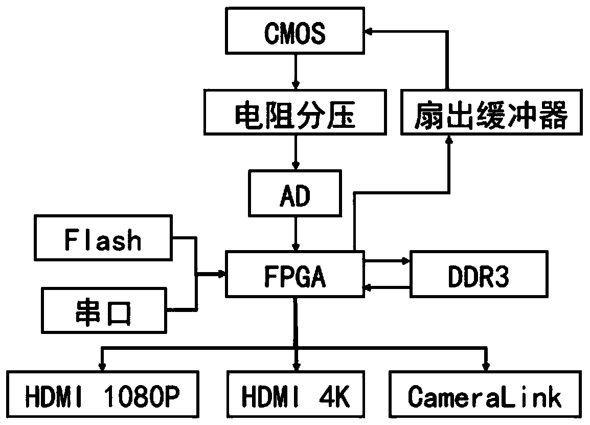
[0074] figure 1 It is a schematic diagram of the system composition of the imaging system. This example uses Xilinx FPGA as the platform. After the system initialization, it is mainly divided into six steps:

[0075] Step 1. The FPGA outputs the driving signal, passes through the fan-out buffer, and then enters the CMOS detector;

[0076] Step 2. The output signal of the CMOS detector enters the high-speed serial AD for analog-to-digital conversion after being divided by resistors;

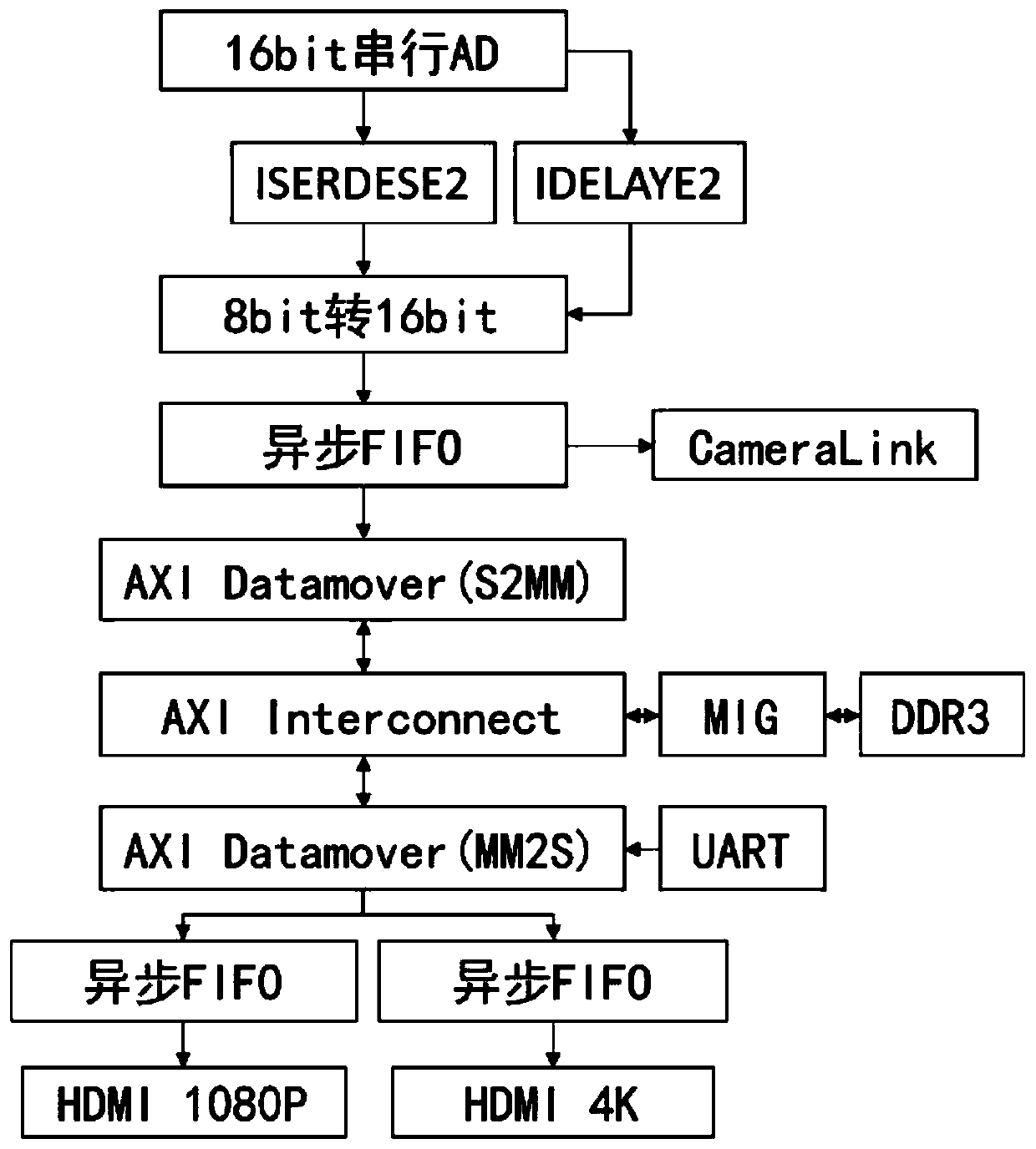
[0077] Step 3. After the FPGA receives the AD data, it performs a serial-to-parallel conversion, and then caches it in DDR3;

[0078] Step 4, the FPGA reads out an image with a resolution of 1920×1080 from the DDR3 according to the frame rate of HDMI 1080P, and outputs it by the HDMI 1080P display circuit;

[0079] Step 5, FPGA reads out an image with a resolution of 4096×2160 from DDR3 according to the frame rate of HDMI 4K, and outputs it by the HDMI 4K display circuit;

[0080] Step 6. The F...


PUM


Abstract

The invention provides an ultrahigh-resolution large-area-array CMOS (complementary metal oxide semiconductor) imaging method, which comprises the following steps that an FPGA (field programmable gatearray) outputs a driving signal, and the driving signal enters a CMOS detector after passing through a fan-out buffer; the CMOS detector outputs a signal, and the signal enters a high-speed serial ADfor analog-to-digital conversion after resistance voltage division; after the FPGA receives the AD data, serial-parallel conversion is carried out, and then the AD data is cached into the DDR3; the FPGA reads an image with the resolution of 1920 * 1080 from the DDR3 according to the frame frequency of the HDMI 1080P, and the image is output by the HDMI 1080P display circuit; the FPGA reads an image with the resolution of 4096 * 2160 from the DDR3 according to the frame frequency of the HDMI 4K, and the image is output by the HDMI 4K display circuit; and the FPGA sends an image with the resolution of 12800 * 12800 according to the time sequence of the Camera Link, and the image is output by the Camera Link display circuit.

Description

technical field [0001] The invention relates to an ultra-high resolution imaging technology, in particular to an ultra-high resolution large area array CMOS imaging method. Background technique [0002] When the surveillance and strike integrated UAV performs an attack mission, it must first rely on the aerial camera to take pictures of the ground before launching missiles for precise strikes. As the eyes of this system, the resolution of the airborne camera plays a vital role in the accuracy of target recognition and strike accuracy. However, at present, the resolution of aviation airborne cameras at home and abroad is generally low, which makes it impossible to track multiple targets at the same time, or even accurately identify an important target. This is a very serious practical problem in the military field. [0003] Aiming at the problem of low resolution, the current common solution abroad is to use multiple cameras to shoot at the same time. This method requires th...

Claims


Application Information

Patent Timeline
Patent Type & Authority Applications(China)
IPC IPC(8): H04N5/374H04N7/01H04N5/765
CPCH04N7/01H04N7/0117H04N7/0125H04N5/765H04N25/76
Inventor 钱芸生池林辉陈益新杨开峰籍宇豪郎怡政刘桂鹏李萍萍张雨程
Owner NANJING UNIV OF SCI & TECH
Why Eureka
Eureka Blog
Learn More