Manufacturing method of heat conduction PCB and PCB
A manufacturing method and technology of heat conductors, applied in the directions of circuit heating devices, multilayer circuit manufacturing, printed circuit manufacturing, etc., can solve problems such as limiting wiring density, prone to wrinkling, and inability to realize circuit manufacturing, so as to eliminate displacement and improve Effect of Overall Routing Density
- Summary
- Abstract
- Description
- Claims
- Application Information
AI Technical Summary
Problems solved by technology
Method used
Image
Examples
Embodiment 1
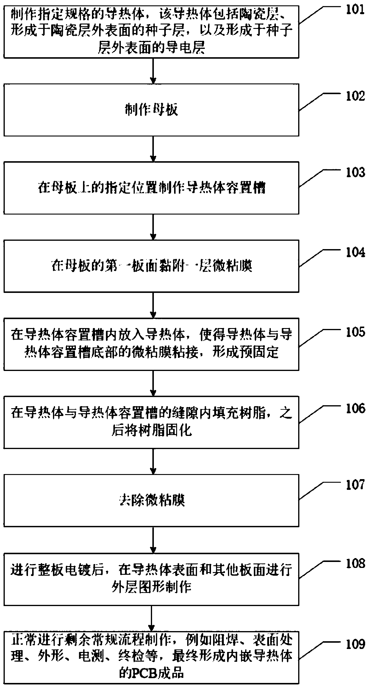
[0040] see image 3 The fabrication method flow chart of shown heat conduction PCB and Figure 4 The schematic diagram of the manufacturing method of the shown heat-conducting PCB, the manufacturing method of the heat-conducting PCB that the embodiment of the present invention provides, comprises:
[0041] Step 101 , making a thermal conductor 8 of specified specifications, the thermal conductor 8 includes a ceramic layer, a seed layer formed on the outer surface of the ceramic layer, and a conductive layer formed on the outer surface of the seed layer.
[0042] The thermal conductor 8 is used to realize the heat dissipation function, and its specific manufacturing method is: first form a seed layer on the upper and lower surfaces of a large ceramic sheet with a certain thickness, and then plate a conductive layer, such as a copper layer, to form a large copper-clad ceramic sheet; The large copper-clad ceramic sheet is divided into several small copper-clad ceramic sheets of ...
Embodiment 2
[0068] see Figure 5 The fabrication method flow chart of shown heat conduction PCB and Figure 6 The schematic diagram of the manufacturing method of the shown heat-conducting PCB, the manufacturing method of the heat-conducting PCB that the embodiment of the present invention provides, comprises:
[0069] Step 201 , making a thermal conductor 8 of specified specifications, the thermal conductor 8 includes a ceramic layer, a seed layer formed on the outer surface of the ceramic layer, and a conductive layer formed on the outer surface of the seed layer.
[0070] Step 202 , making the motherboard 5 .
[0071] Step 203 , making a thermal conductor accommodating groove 6 at a designated position on the motherboard 5 .
[0072] Step 204 , adhering a layer of micro-mucosa 7 on the first surface of the motherboard 5 .
[0073] Step 205, pre-filling the specified amount of resin 9 in the heat conductor storage tank 6, and then putting the heat conductor 8 into the heat conductor ...
Embodiment 3
[0082] This embodiment provides a PCB, which is manufactured according to the manufacturing method described in the first or second embodiment above. Since the embedded heat conductor 8 includes a ceramic layer and a conductive layer formed on the outer surface through the seed layer, the outer layer graphics can be made on the surface of the heat conductor 8 at the same time, which improves the wiring density of the PCB product.
PUM
 Abstract
Description
Claims
Application Information


