Internal Error Calibration Compensation System and Calibration Compensation Method of Photon Interference Imaging System

A technology of interference imaging and error calibration, applied in the field of optical interference imaging, can solve problems such as device errors and affecting imaging system performance, and achieve the effects of reducing volume, improving imaging quality, and improving reliability and stability

Active Publication Date: 2021-08-24
CHANGCHUN INST OF OPTICS FINE MECHANICS & PHYSICS CHINESE ACAD OF SCI
View PDF4 Cites 0 Cited by
  • Summary
  • Abstract
  • Description
  • Claims
  • Application Information

AI Technical Summary

Problems solved by technology

[0008] The present invention provides a calibration compensation system and a calibration compensation method for the internal errors of the photon interference imaging system in order to solve the problems that there are various errors inside the devices of the existing interference imaging system, which further affect the performance of the imaging system.

Method used


Image

  • Internal Error Calibration Compensation System and Calibration Compensation Method of Photon Interference Imaging System
  • Internal Error Calibration Compensation System and Calibration Compensation Method of Photon Interference Imaging System
  • Internal Error Calibration Compensation System and Calibration Compensation Method of Photon Interference Imaging System

Examples


specific Embodiment approach 1

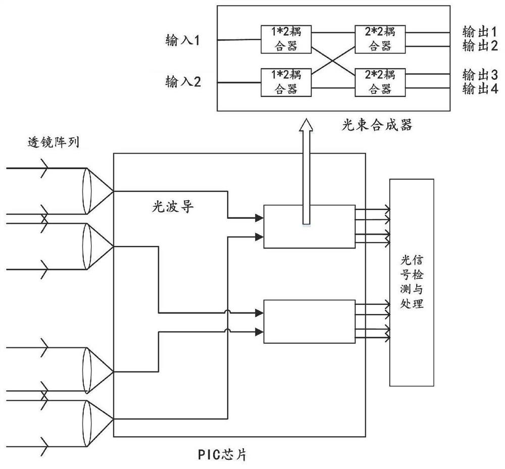
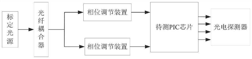
[0034] Specific implementation mode 1. Combination figure 2Description of this embodiment, the internal error calibration and compensation system of the photon interference imaging system includes a calibration light source (thorlab 1550nm infrared laser), a phase adjustment device (general photonics electronic delay line), a PIC chip to be tested, and a light intensity detection device (short-wave infrared camera) , 1*2 fiber optic coupler, fiber optic jumper, etc. The PIC chip to be tested has two input ports and four output ports. The interior only includes a set of interferometers, which are composed of a pair of waveguides and a beam combiner. The waveguide mainly transmits light and adjusts the optical path. The beam combiner performs interference and completes the sampling of the fringes at quarter-period intervals.

[0035] One end of the optical fiber coupler is connected to the calibration light source, so that the calibration light source is divided into two outpu...

specific Embodiment approach 2

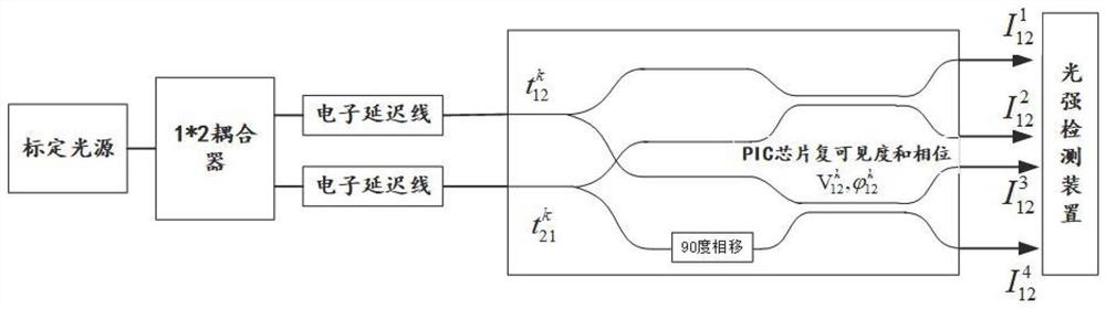
[0037] Specific embodiment two, combine image 3 Describe this implementation mode, this implementation is the calibration compensation method of the internal error calibration compensation system of the photon interference imaging system described in the specific implementation mode 1, establish a mathematical model of the PIC photonic integrated chip, calibrate the internal error of the system, and then re-image During the construction process, the calibration data is used to compensate for the error. By adopting a phase-locked dual light source calibration compensation method, and by controlling the light intensity and phase difference of the calibration light source, the high-precision error calibration compensation of the PIC chip to be tested is realized. This method adopts phase-locked dual light source calibration compensation, which is realized by the following steps:

[0038] 1. Establish a mathematical model of the input and output of the PIC chip to be tested. The...


PUM


Abstract

The internal error calibration compensation system and calibration compensation method of the photon interference imaging system relate to the field of optical interference imaging technology, and solve the problems that various errors exist in the devices of the existing interference imaging system, which in turn affect the performance of the imaging system, including calibration of the light source and phase adjustment. device, a PIC chip to be tested, a light intensity detection device, and a fiber coupler; one end of the fiber coupler is connected to a calibration light source, and the calibration light source is divided into two outputs, and each of the two output ports at the other end of the fiber coupler is connected to a phase The input port of the adjustment device is connected, and the output ports of the two phase adjustment devices are respectively connected to the two input ports of the PIC chip to be tested; the light intensity detection device is placed at the back end of the PIC chip to be tested, and is used to detect the four output ports of the PIC chip output light intensity. For the internal error of the PIC integrated chip, the invention effectively corrects the internal error by establishing an error calibration compensation model, so that the system can achieve better imaging effect. Simplify system operation.

Description

technical field [0001] The invention relates to the technical field of optical interference imaging, in particular to an internal error calibration compensation system and calibration compensation method of a photon interference imaging system. Background technique [0002] The core of photonic integrated interference imaging is the PIC photonic integrated chip. The PIC photonic integrated chip adopts integrated optical technology, which enables the device to maintain reliability and stability while greatly reducing the volume, and improves the performance of the device as a whole. Due to the complex internal structure of the device, it contains many structural units. Therefore, PIC photonic integrated chips are prone to errors during the manufacturing process, and once the chip is packaged and manufactured, the errors cannot be eliminated by hardware correction. Therefore, there is a need for a method that can learn the internal error of the photonic integrated chip, and ...

Claims


Application Information

Patent Timeline
Patent Type & Authority Patents(China)
IPC IPC(8): G01J3/28G01J3/02
CPCG01J3/0259G01J3/0297G01J3/2803G01J3/2823
Inventor 张怡王越刘欣悦孟浩然刘欣然樊元朋
Owner CHANGCHUN INST OF OPTICS FINE MECHANICS & PHYSICS CHINESE ACAD OF SCI
Why Eureka
Try Eureka