A kind of all-inorganic solid-state electrochromic device and preparation method thereof

An electrochromic device and electrochromic layer technology, which can be used in instruments, nonlinear optics, optics, etc., and can solve the problems of slow color changing response speed, high production cost, and inability to meet the requirements of industrial use.

Active Publication Date: 2022-07-08
ZHONGBEI UNIV
View PDF5 Cites 0 Cited by
  • Summary
  • Abstract
  • Description
  • Claims
  • Application Information

AI Technical Summary

Problems solved by technology

Due to the defects in the performance of each film layer, the traditional electrochromic device has defects such as short cycle life, slow response speed of discoloration, unstable performance, high production cost and complicated process.
Domestic electrochromic research mainly focuses on the performance improvement of single-layer electrochromic thin film materials and the preparation of small-sized semi-solid devices and a small amount of all-solid-state devices, and the cycle life of the devices can only reach about a few thousand times. , far from reaching the 10 required for industrial use 4 More than times

Method used


Image

  • A kind of all-inorganic solid-state electrochromic device and preparation method thereof
  • A kind of all-inorganic solid-state electrochromic device and preparation method thereof
  • A kind of all-inorganic solid-state electrochromic device and preparation method thereof

Examples


Embodiment Construction

[0025] The present invention will be described in detail below with reference to specific embodiments. The following examples will help those skilled in the art to further understand the present invention, but do not limit the present invention in any form. It should be noted that, for those skilled in the art, several modifications and improvements can be made without departing from the concept of the present invention. These all belong to the protection scope of the present invention.

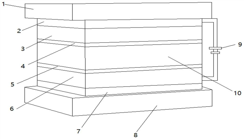
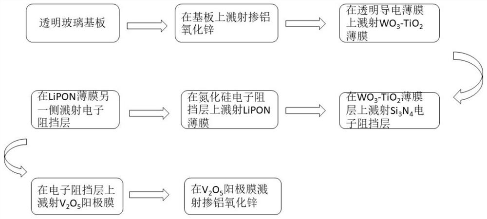
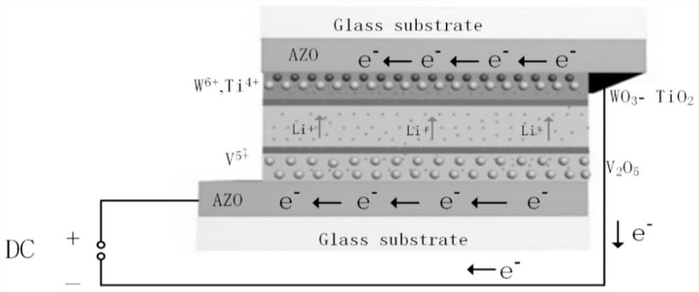
[0026] like figure 1 As shown, the embodiment of the present invention provides an all-inorganic solid-state electrochromic device, comprising a transparent glass substrate A1 and a transparent glass substrate B8 arranged on both sides, and a transparent conductive substrate A1 arranged on the transparent glass substrate A1 close to the middle The thin film layer I2 is arranged on the transparent glass substrate B near the transparent conductive thin film layer II7 in the middle, the electr...


PUM

PropertyMeasurementUnit
thicknessaaaaaaaaaa
diameteraaaaaaaaaa
thicknessaaaaaaaaaa

Abstract

The invention discloses an all-inorganic solid-state electrochromic device, comprising a transparent glass substrate A and a transparent glass substrate B arranged on both sides, a transparent conductive thin film layer I arranged on the transparent glass substrate A near the middle, and arranged on the transparent glass The transparent conductive film layer II near the middle of the substrate B, the electrochromic layer disposed inside the transparent conductive film layer I, the ion storage layer disposed inside the transparent conductive film layer II, and the electron blocking layer disposed inside the electrochromic layer Layer I, the electron blocking layer II arranged on the inner side of the ion storage layer; the ion transport layer arranged between the electron blocking layer I and the electron blocking layer II; the electrochromic layer adopts WO 3 Doped TiO 2 film, the ion transport layer adopts lithium phosphorus oxynitride (LiPON) film, and the ion storage layer adopts V 2 O 5 The thin film of the invention solves the defects of unstable discoloration performance and poor cycle life that have always existed in the process of cyclic use of electrochromic devices.

Description

technical field [0001] The invention relates to the field of electrochromic devices, in particular to an all-inorganic solid-state electrochromic device and a preparation method thereof. Background technique [0002] Electrochromic means that under the action of external electric field, electrochromic film can achieve the effect of coloring and bleaching. Its excellent display effect is widely used in electronic information, sensors, smart windows, military and national defense and other fields. Traditional electrochromic devices have defects such as short cycle life, slow discoloration response speed, unstable performance, high production cost, and complicated process due to the defects in the performance of each film layer. Domestic electrochromic research mainly focuses on the performance improvement of single-layer electrochromic thin film materials, the preparation of small-sized semi-solid-state devices, and the preparation of a small number of all-solid-state devices,...

Claims


Application Information

Patent Timeline
Patent Type & Authority Patents(China)
IPC IPC(8): G02F1/1523G02F1/153
CPCG02F1/1523G02F1/1533
Inventor 李晨贾鹏宇洪应平熊继军
Owner ZHONGBEI UNIV
Why Eureka
Try Eureka