Check patentability & draft patents in minutes with Patsnap Eureka AI!

OCA film encapsulation process for a display module

A display module and thin film packaging technology, applied in semiconductor devices, electrical components, circuits, etc., can solve the problems of low production efficiency, difficult to meet production needs, and high equipment, so as to improve the packaging effect, meet production needs, and reduce production costs. Effect

Active Publication Date: 2020-08-11
AET DISPLAY LTD +1
View PDF4 Cites 0 Cited by
  • Summary
  • Abstract
  • Description
  • Claims
  • Application Information

AI Technical Summary

Problems solved by technology

However, this packaging method has high requirements on equipment and technology, and the production efficiency is low, so it is difficult to meet the production demand.

Method used


Image

  • OCA film encapsulation process for a display module
  • OCA film encapsulation process for a display module
  • OCA film encapsulation process for a display module

Examples


no. 1 example

[0035] The first embodiment provided by the present invention is an OCA film packaging process for a display module, which includes the following steps:

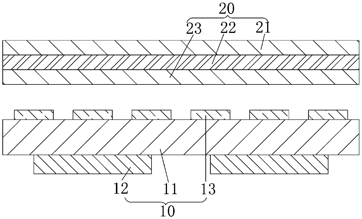
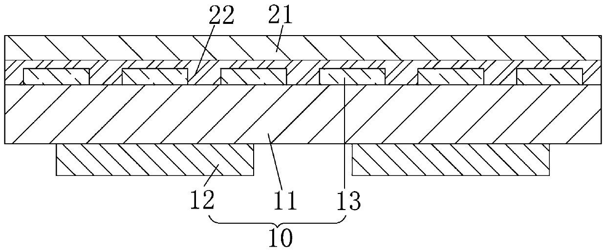
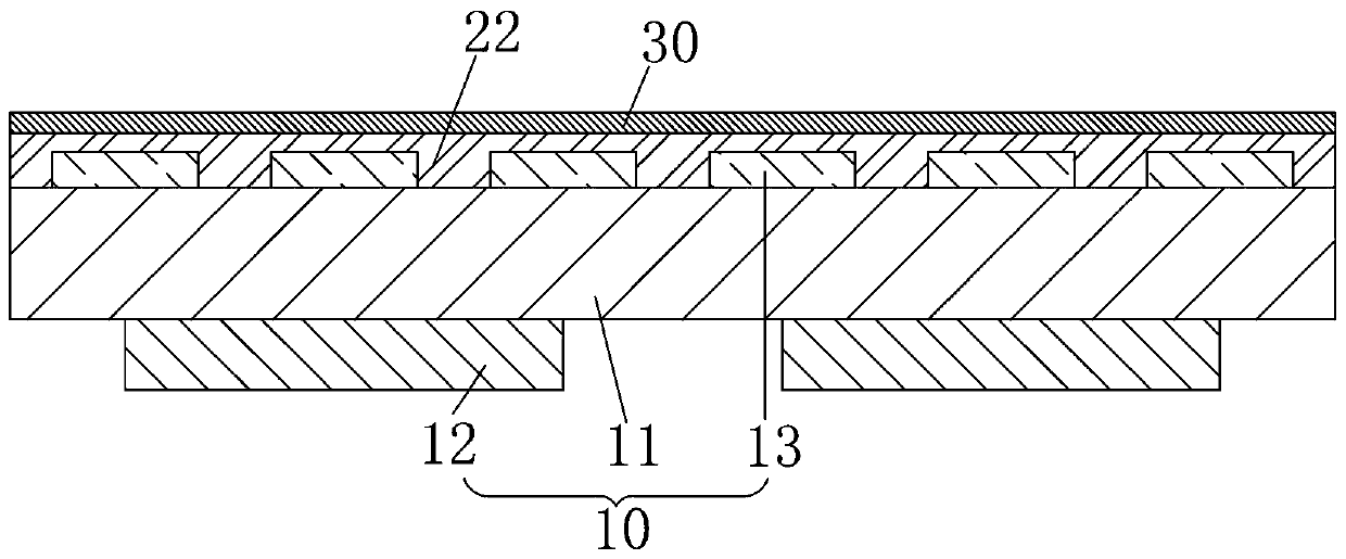
[0036] (1) if figure 1 As shown, a display module 10 is provided, and the display module 10 includes a display substrate 11, a driver IC 12 and an LED chip 13; a plurality of driver ICs 12 are mounted on the bottom surface of the display substrate 11, and a plurality of LED chips 13 are mounted on the display substrate 11 top surface. Wherein, the display substrate 11 is a rigid printed circuit board.

[0037] (2) if figure 1 As shown, an OCA optical adhesive 20 is provided, and the OCA optical adhesive 20 includes an upper release film 21 , an optical adhesive 22 and a lower release film 23 that are laminated sequentially from top to bottom. Wherein, the optical colloid 22 is acrylic and transparent colloid.

[0038] (3) Tear off the lower release film 23, and attach the bottom surface of the optical colloid 22 to the t...

no. 2 example

[0042] The second embodiment provided by the present invention is an OCA film packaging process for a display module, which includes the following steps:

[0043] (1) if figure 1 As shown, a display module 10 is provided, and the display module 10 includes a display substrate 11, a driver IC 12 and an LED chip 13; a plurality of driver ICs 12 are mounted on the bottom surface of the display substrate 11, and a plurality of LED chips 13 are mounted on the display substrate 11 top surface. Wherein, the display substrate 11 is a rigid printed circuit board.

[0044] (2) if figure 1 As shown, an OCA optical adhesive 20 is provided, and the OCA optical adhesive 20 includes an upper release film 21 , an optical adhesive 22 and a lower release film 23 that are laminated sequentially from top to bottom. Wherein, the optical colloid 22 is acrylic and transparent colloid.

[0045] (3) Tear off the lower release film 23, and attach the bottom surface of the optical colloid 22 to the ...


PUM


Abstract

The invention provides an OCA film packaging process of a display module, comprising the following steps: (1) providing a display module; (2) providing OCA (Optically Clear Adhesive); (3) tearing offa lower release film, attaching the bottom surface of an optical colloid to the top surface of an LED chip, and pressing down the top surface of an upper release film by using a jig to enable the bottom surface of the optical colloid to be attached to the top surface of a display substrate and coat the LED chip; (4) providing a light guide film, tearing off the upper release film, attaching the bottom surface of the light guide film to the top surface of the optical colloid, and pressing down the top surface of the light guide film by using a jig to enable the bottom surface of the light guidefilm to be attached to the top surface of the optical colloid; and (5) curing the optical colloid to obtain a single-layer packaged display module. The OCA packaging process is mainly a laminating process, the steps are few and simple, and the technology of automatic laminating equipment is mature. Therefore, high-efficiency packaging can be realized, the production requirement can be met, and the production cost can be reduced.

Description

technical field [0001] The invention relates to the technical field of LED display, in particular to an OCA film packaging process of a display module. Background technique [0002] LED displays include small-pitch LED displays, mini LED displays, and micro LED displays. The structure of the LED display is usually that multiple independent display modules are spliced ​​through mechanical components to form a large-sized LED display. [0003] The display module includes a PCB board, a plurality of LED chips mounted in a rectangular array on one side of the PCB board, and IC components arranged on the other side of the PCB board. In order to prevent the LED chip from being directly exposed to the air, easily polluted or artificially damaged, affecting or destroying the function of the chip, it is usually necessary to pot the side of the PCB board where the LED chip is mounted with a layer of epoxy resin, and the epoxy resin will bond the LED chip and The bonding wires are en...

Claims


Application Information

Patent Timeline
Patent Type & Authority Patents(China)
IPC IPC(8): H01L25/16H01L25/00H01L21/56
CPCH01L21/56H01L25/167H01L25/50
Inventor 梁文骥许晋彰赵春雷孙明
Owner AET DISPLAY LTD
Features
  • R&D
  • Intellectual Property
  • Life Sciences
  • Materials
  • Tech Scout
  • Unparalleled Data Quality
  • Higher Quality Content
  • 60% Fewer Hallucinations
Learn More