Stamp hole bonding pad surface mounting type image visual processing module

A surface mount, image vision technology, applied in the field of image processing, to achieve the effect of improving stability, good portability, and improving signal quality

Pending Publication Date: 2020-01-07
深圳市猫头鹰微视科技有限公司
View PDF0 Cites 0 Cited by
  • Summary
  • Abstract
  • Description
  • Claims
  • Application Information

AI Technical Summary

Problems solved by technology

At present, the modules in the industry market are basically customized requirements, which cannot solve the above problems well, and have great limitations.

Method used


Image

  • Stamp hole bonding pad surface mounting type image visual processing module
  • Stamp hole bonding pad surface mounting type image visual processing module
  • Stamp hole bonding pad surface mounting type image visual processing module

Examples


no. 1 example

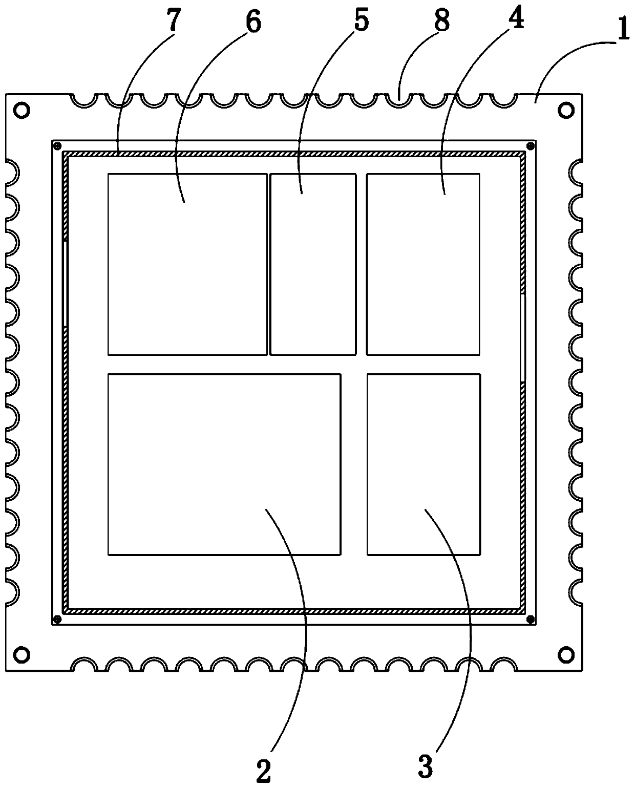
[0045] Please refer to Figure 1-Figure 4 , in the first embodiment of the invention:

[0046] Stamp hole pad surface mount type image vision processing module includes:

[0047] PCB substrate 1;

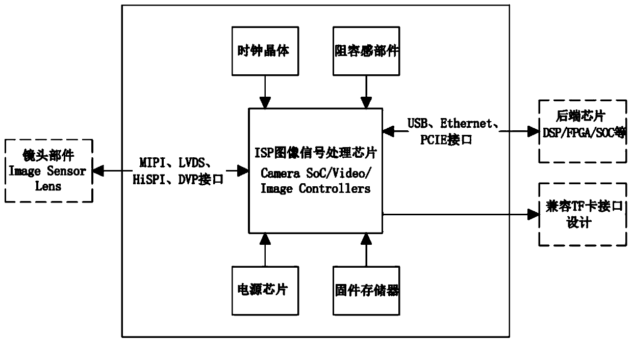
[0048] ISP image processing chip 2, the ISP image processing chip 2 is installed on the top of the PCB substrate 1;

[0049] A resistance-capacitance sensing component 3, the resistance-capacitance sensing component 3 is installed on the top of the PCB substrate 1;

[0050] A power chip 4, the power chip 4 is mounted on the top of the PCB substrate 1;

[0051] A clock crystal 5, the clock crystal 5 is mounted on the top of the PCB substrate 1;

[0052] A firmware memory 6, the firmware memory 6 is mounted on the top of the PCB substrate 1 .

[0053] The ISP image processing chip 2 includes Camera SoC, Video, Image Controllers chips with image signal and media services.

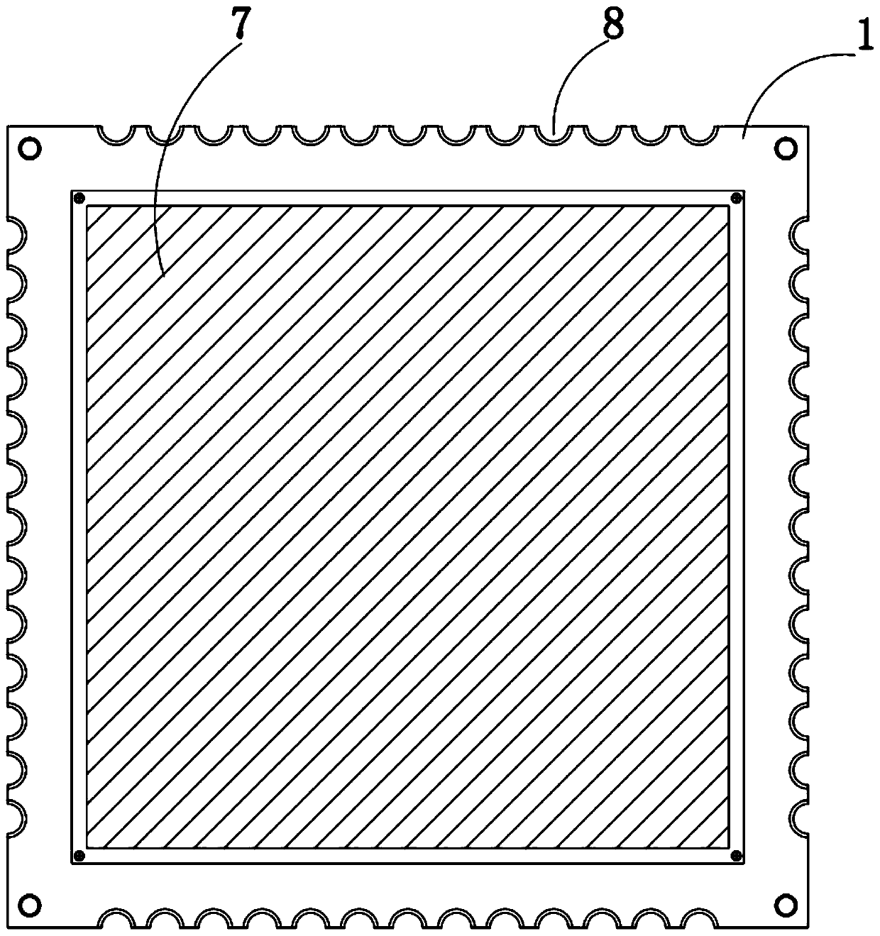
[0054] A shielding case 7 is fixedly mounted on the top of the PCB substrate 1 .

[0055] The four sides of ...

no. 2 example

[0071] Please refer to Figure 5-6 The difference between this embodiment and the first embodiment is that a camera connector 9 is installed on the PCB substrate 1, the camera connector 9 is located in the shield 7, and the shield 7 is provided with an avoidance hole 11 , and the avoidance hole 11 is adapted to the camera connector 9, and the camera connector 9 is used for connecting external lens components.

no. 3 example

[0073] Please refer to Figure 7 The only difference between this embodiment and the first embodiment is that the PCB design of the PCB substrate 1 adopts a large copper pad 11 exposed at the bottom of the substrate.


PUM


Abstract

The invention provides a stamp hole bonding pad surface mounting type image visual processing module. The stamp hole bonding pad surface mounting type image visual processing module comprises a PCB substrate; an ISP image processing chip, wherein the ISP image processing chip is installed on the PCB substrate; a resistance-capacitance-inductance component installed on the PCB substrate, a power supply chip, wherein the power supply chip is installed on the PCB substrate; a clock crystal, wherein the clock crystal is installed on the PCB substrate; and a firmware memory, wherein the firmware memory is installed on the PCB substrate. The stamp hole bonding pad surface mounting type image visual processing module provided by the invention has the advantages of low cost, high hardware integration level, high compatibility, high software integration level, more intelligent module and capability of reducing the use threshold of customers.

Description

technical field [0001] The invention relates to the technical field of image processing, in particular to a stamp hole pad surface mount type image vision processing module. Background technique [0002] With the current development of artificial intelligence AI, AIOT, and 5G technology, the application scenarios of image vision are becoming more and more popular. The industry market puts forward high integration requirements for the hardware and software dimensions of image processing. Integrated modules facilitate the rapid development of end customers. , It is convenient for embedding and product terminals, it is convenient for improving the consistency and stability of image quality, it is convenient for the development of multiple image requirements, and it is convenient for the protection of intellectual property rights. [0003] From the perspective of product hardware design, based on the current common phenomenon in the industry, the hardware design of terminal prod...

Claims


Application Information

Patent Timeline
Patent Type & Authority Applications(China)
IPC IPC(8): H04N5/225H04N5/232H01L27/146
CPCH01L27/14634H01L27/14636H04N23/55H04N23/54H04N23/80
Inventor 武浩
Owner 深圳市猫头鹰微视科技有限公司
Why Eureka
Try Eureka