Packaging structure, finished circuit board, electronic device, electronic equipment and soldering method
A technology for packaging structure and electronic devices, which is applied in the direction of electrical components, assembling printed circuits with electrical components, printed circuits, etc.
- Summary
- Abstract
- Description
- Claims
- Application Information
AI Technical Summary
Problems solved by technology
Method used
Image

Examples
Embodiment Construction
[0063] In order to make the technical solutions of the embodiments of the present application clearer, the terms involved in the embodiments of the present application are explained first.
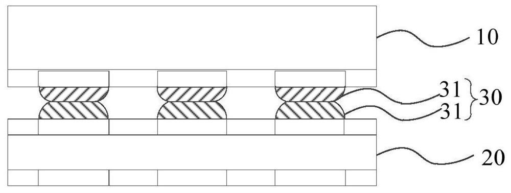
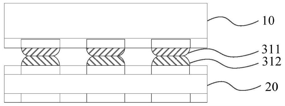
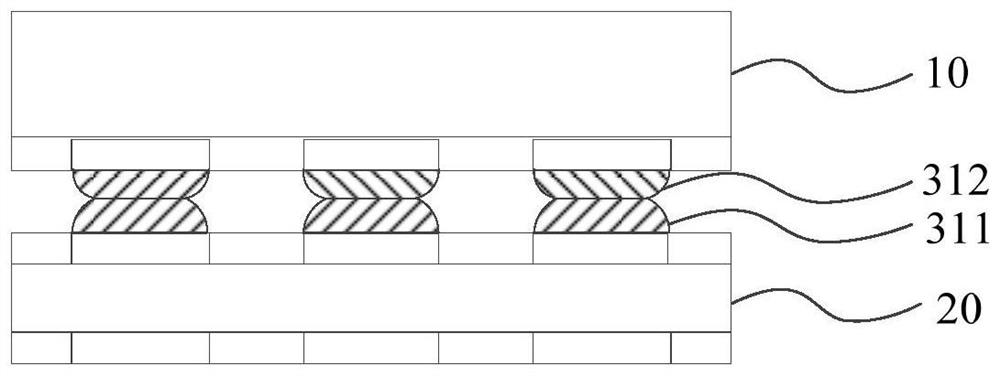
[0064] PCB (Printed Circuit Board), the Chinese name is printed circuit board, also known as printed circuit board, is an important electronic component, a support for electronic devices, and a carrier for electrical connections of electronic devices. Because it is made using electronic printing, it is called a "printed" circuit board.
[0065] PCBA (Printed Circuit Board+Assembly), the Chinese name is the finished circuit board, which assembles various electronic devices on the circuit board through the surface packaging process to form a finished circuit board.
[0066] SiP (System in Package) packaging is a commonly used method for miniaturization of packaging devices. SiP packaging is to preferentially assemble multiple active electronic components with different functions and optiona...
PUM
 Abstract
Description
Claims
Application Information
 - R&D
- Intellectual Property
- Life Sciences
- Materials
- Tech Scout
- Unparalleled Data Quality
- Higher Quality Content
- 60% Fewer Hallucinations
Browse by: Latest US Patents, China's latest patents, Technical Efficacy Thesaurus, Application Domain, Technology Topic, Popular Technical Reports.
© 2025 PatSnap. All rights reserved.Legal|Privacy policy|Modern Slavery Act Transparency Statement|Sitemap|About US| Contact US: help@patsnap.com