Embedded memory

An embedded memory and embedded technology, which is applied in the field of memory, can solve problems such as increased packaging burden, excessive memory space occupation, and signal crosstalk, and achieve the effects of reducing workload, reducing signal crosstalk, and saving costs

Active Publication Date: 2020-01-14
YANGTZE MEMORY TECH CO LTD
View PDF5 Cites 0 Cited by
  • Summary
  • Abstract
  • Description
  • Claims
  • Application Information

AI Technical Summary

Problems solved by technology

In actual use, in order to increase the storage capacity of the embedded memory, it is often necessary to expand the embedded memory, but now it is becoming more and more difficult to expand the capacity of the embedded memory. The existing expansion method is to increase the embedded format Flash memory structure or number of products, as attached figure 2 As shown, a plurality of corresponding controllers 13 in a plurality of embedded flash memory structures or products 12 are respectively connected to the main processor 11 through a plurality of embedded interfaces, which will increase the burden (load) of the main processor and easily cause Signal crosstalk (crosstalk)
In addition, due to the increase of embedded flash memory structures or products, the memory space is too occupied, which takes up additional space and increases the packaging burden

Method used


Image

  • Embedded memory
  • Embedded memory
  • Embedded memory

Examples


Embodiment 1

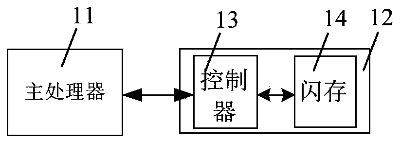
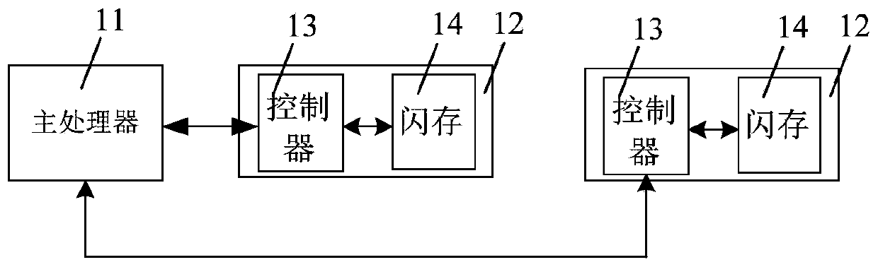
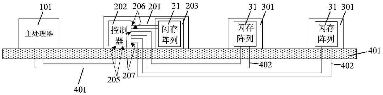
[0039] image 3 It is a schematic structural diagram of an embedded memory according to an embodiment of the present invention.

[0040] refer to image 3, the embedded memory of this embodiment includes: a main processor 101, an embedded flash memory structure 201, and several second bare flash memory structures 301, wherein the embedded flash memory structure 201 includes a controller 202 and several first bare flash memory structures 203, the plurality of first bare flash memory structures 203 have a flash memory array 21, and the plurality of second bare flash memory structures 301 each have a flash memory array 31, the controller 202 includes a plurality of input terminals 205 and a plurality of output terminals, the Several output terminals 206 include embedded output terminals 206 and non-embedded output terminals 207, and the embedded output terminals 206 are connected to the flash memory arrays 21 in the plurality of first bare flash memory structures 203;

[0041] ...


PUM


Abstract

An embedded memory includes: a main processor; an embedded flash memory structure; a plurality of second bare flash memory structures. The embedded flash memory structure comprises a controller and aplurality of first bare flash memory structures; flash memory arrays are arranged in the plurality of first bare flash memory structures and the plurality of second bare flash memory structures; the controller comprises a plurality of input ends and a plurality of output ends; the plurality of output ends comprise a plurality of embedded output ends and a plurality of non-embedded output ends; theplurality of embedded output ends are connected with the flash memory arrays in the plurality of first bare flash memory structures; the main processor is connected with part of the input ends of thecontroller in the embedded flash memory structure; and the flash memory arrays in the plurality of second bare flash memory structures are correspondingly connected with the non-embedded output endsof the controller in the embedded flash memory structure. When the embedded memory is expanded, the workload of the main processor can be reduced, and the signal crosstalk of the main processor end can be reduced; only one controller is needed, so that the cost is saved.

Description

technical field [0001] The invention relates to the field of memory, in particular to an embedded memory. Background technique [0002] NAND flash memory is a better storage device than hard disk drives, and it has been widely used in electronic products as people pursue non-volatile storage products with low power consumption, light weight and high performance. [0003] After the 3D NAND memory is manufactured, it is generally necessary to divide the wafer to form several discrete NAND flash memory structures, and then it is necessary to bind the NAND flash memory structure and the main processor on the PCB board and connect the two through the metal lines on the PCB board. Or connect to form embedded memory, according to the difference of interface mode, described embedded memory comprises eMMC (embedded Multi Media Card) memory, UFS (Universal Flash Storage) memory and BGA SSD (Ball Grid Array SSD) memory. [0004] In the actual memory product, the embedded flash memory ...

Claims


Application Information

Patent Timeline
Patent Type & Authority Applications(China)
IPC IPC(8): H01L27/1157G11C16/14
CPCG11C16/14H10B43/35
Inventor 武泽翰曹永赞
Owner YANGTZE MEMORY TECH CO LTD
Why Eureka
Try Eureka