Non-direct electrical contact orientation ordered nLED light-emitting display device

A light-emitting display device and electrical contact technology, applied in the direction of electric solid-state devices, electrical components, semiconductor devices, etc., can solve problems such as difficult operation of chips, avoid complex bonding, reduce production cycle and production costs, and reduce the complexity of the production process degree of effect

Active Publication Date: 2020-01-14
FUZHOU UNIVERSITY
View PDF3 Cites 4 Cited by
  • Summary
  • Abstract
  • Description
  • Claims
  • Application Information

AI Technical Summary

Problems solved by technology

However, when the size of the LED chip is small to a certain extent, the operation of the chip becomes more and more difficult, especially for nLED grains, how to orderly transfer the grains with different luminescent color

Method used


Image

  • Non-direct electrical contact orientation ordered nLED light-emitting display device
  • Non-direct electrical contact orientation ordered nLED light-emitting display device

Examples


Embodiment Construction

[0018] The present invention will be further described below with reference to the accompanying drawings and embodiments.

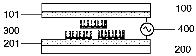
[0019] Please refer to figure 1 The invention provides a non-direct electrical contact orientation ordered nLED light-emitting display device, comprising an upper driving electrode substrate, an upper driving electrode, a nano-LED chip, a lower driving electrode and a lower driving electrode substrate arranged in sequence from top to bottom; An AC drive control module is also provided, and the two ends of the AC drive control module are respectively connected to the upper drive electrode and the lower drive electrode; the nano-LED die sheet is made up of several nano-LED die arranged in an orderly manner, which is guaranteed to be placed on the electrodes. When between the substrates, the light-emitting layer of each nano-LED crystal grain is parallel to the electrode substrate and perpendicular to the direction of the electric field; the driving electrod...


PUM

PropertyMeasurementUnit
Horizontal sizeaaaaaaaaaa
Vertical sizeaaaaaaaaaa
Thicknessaaaaaaaaaa

Abstract

The invention relates to a non-direct electrical contact orientation ordered nLED light-emitting display device. The device comprises in order from top to bottom: an upper driving electrode substrate,an upper driving electrode, a nano LED crystal grain sheet, a lower driving electrode and a lower driving electrode substrate. The device further comprises an alternating-current driving control module, the two ends of the alternating-current driving control module are respectively connected with the upper driving electrode and the lower driving electrode, the nano LED crystal grain sheet is formed by orderly arranging a plurality of nano LED crystal grains, so that when the nano LED crystal grain sheet is placed between the electrode substrates, and the light-emitting layer of each nano LEDcrystal grain is parallel to the electrode substrates and is perpendicular to the direction of an electric field; and at least one of the upper driving electrode and the lower driving electrode is isolated from the nano LED crystal grains through an insulating dielectric layer, and the nano LED crystal grains are lightened through electromagnetic coupling under an alternating driving signal. According to the invention, an indirect electrical contact method is adopted to achieve ordered nLED light-emitting display, a huge transfer process of micron-scale and nano-scale LEDs can be omitted, andthe process cost is effectively reduced.

Description

technical field [0001] The present invention and the field of integrated semiconductor light-emitting and display, in particular, relate to a non-direct electrical contact orientation ordered nLED light-emitting display device. Background technique [0002] LED display has the advantages of self-illumination, high brightness and luminous efficiency, low power consumption, high stability, etc., and is widely used in various occasions. With the reduction of LED chip size and pixel pitch, LED display is expected to achieve flexible, highly transparent, interactive, and modular splicing display, which is considered to be a revolutionary display technology with full functions and applications. Among them, μLED display is a new type of display technology consisting of an array of micron-scale LED light-emitting pixels, and nLED (nano LED) display is a new type of display technology consisting of an array of nano-scale LED light-emitting pixels. At present, major domestic and fore...

Claims


Application Information

Patent Timeline
IPC IPC(8): H01L27/15H01L33/62B82Y40/00
CPCH01L27/153H01L33/62B82Y40/00H01L27/156H01L33/08H01L25/0753H01L25/167
Inventor 周雄图陈桂雄郭太良张永爱吴朝兴林志贤严群
Owner FUZHOU UNIVERSITY
Why Eureka
Try Eureka