A nled pixel setting and repair method

A repair method and pixel technology, applied in identification devices, static indicators, instruments, etc., can solve the problems of difficult chip operation, difficult pixel defect monitoring and repair, and low device yield.

Active Publication Date: 2021-07-06
FUZHOU UNIV +1
View PDF19 Cites 0 Cited by
  • Summary
  • Abstract
  • Description
  • Claims
  • Application Information

AI Technical Summary

Problems solved by technology

However, when the LED chip size is small to a certain extent, the operation of the chip will become more and more difficult
In traditional μLED display, each luminous pixel contains a μLED chip, and the cathode and anode of each chip are respectively connected and bonded to the pixel electrodes of the drive backplane in an orderly manner through massive transfer and precise alignment. The technical links such as alignment and bonding with electrodes are extremely demanding, the device yield rate is low, and pixel defect monitoring and repair are extremely difficult, which seriously hinders the commercialization of μLED displays

Method used


Image

  • A nled pixel setting and repair method
  • A nled pixel setting and repair method

Examples


Embodiment 1

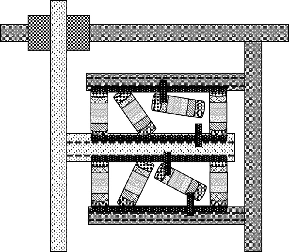
[0039] Please refer to figure 1 and figure 2 , the present invention discloses an NLED electrode arrangement scheme and interconnection method, each light-emitting pixel unit includes 8 NLED chips; the n-electrode of the NLED chip is provided with a first electrode interconnection region 301 of an n-type semiconductor and an n-type semiconductor The first electrode spare area 302 of the p-electrode is provided with the second electrode spare area 701 of the p-type semiconductor and the second electrode interconnection area 702 of the p-type semiconductor; the cathode of the driving backplane is provided with the cathode interconnection area 12 and the cathode spare area 13. The anode of the driving backplane is also provided with an anode interconnection area 9 and an anode spare area 10; the transfer arrangement of the NLED chip in the pixel area adopts electrophoresis; the interconnection mode of the NLED chip electrode and the pixel electrode of the driving backplane is: ...


PUM

PropertyMeasurementUnit
sizeaaaaaaaaaa
sizeaaaaaaaaaa
sizeaaaaaaaaaa

Abstract

The invention relates to an NLED pixel setting and repairing method. Each light-emitting pixel unit includes n NLED chips, and each pixel unit includes at least m NLED light emitters; the NLED chip electrode and the driving backplane electrode are all provided with an interconnection area and a spare area, through Au-In bonding, After the interconnection area of ​​the NLED chip electrode is connected to the interconnection area of ​​the pixel electrode on the driving backplane by a composite method of non-Au-In interconnection or Au-In bonding and non-Au-In interconnection, the electrode area is monitored in real time For detection, the NLED chip electrode spare area is connected to the corresponding spare area of ​​the drive backplane electrode by in-situ non-Au-In connection in the corresponding defective area for repair, without removing the NLED chip with unreliable bonding and connection. The invention effectively reduces the production cycle and production cost of the LED device, and greatly improves the yield rate of the LED display device.

Description

technical field [0001] The invention relates to the field of integrated semiconductor lighting and display, in particular to an NLED pixel setting and repairing method. Background technique [0002] LED displays have the advantages of self-illumination, high brightness and luminous efficiency, low power consumption, high stability, etc., and are widely used in various occasions. With the reduction of LED chip size and pixel pitch, LED display is expected to realize flexible, highly transparent, interactive and modular splicing display, which is considered to be a revolutionary display technology with full functions and full application fields. μLED display is a new type of display technology composed of arrays of micron-scale LED light-emitting pixels, and NLED (Nano-LED) display is a new type of display technology composed of arrays of nano-scale LED light-emitting pixels. NLED can adjust the emission wavelength by changing the diameter, which has potential application pro...

Claims


Application Information

Patent Timeline
Patent Type & Authority Patents(China)
IPC IPC(8): G09F9/33G09F9/302G09G3/00
CPCG09F9/302G09F9/33G09G3/006
Inventor 周雄图翁雅恋郭太良张永爱吴朝兴林志贤严群
Owner FUZHOU UNIV
Why Eureka
Try Eureka