Preparation method of semiconductor device

A semiconductor and device technology, which is applied in the field of semiconductor device preparation, can solve the problems of more exposure and etching times, increased manufacturing costs, and low manufacturing speed of semiconductor devices, so as to reduce the number of times of deposition and etching , the effect of increasing the formation speed

Active Publication Date: 2020-01-17
YANGTZE MEMORY TECH CO LTD
View PDF3 Cites 0 Cited by
  • Summary
  • Abstract
  • Description
  • Claims
  • Application Information

AI Technical Summary

Problems solved by technology

[0004] The invention provides a method for preparing a semiconductor device to solve the technical problems that the manufacturing speed of the semiconductor device is low and the manufacturing cost is increased due to the high number of times of exposure and etching

Method used


Image

  • Preparation method of semiconductor device
  • Preparation method of semiconductor device
  • Preparation method of semiconductor device

Examples


Embodiment Construction

[0047] The following are preferred embodiments of the present invention. It should be pointed out that for those skilled in the art, without departing from the principle of the present invention, some improvements and modifications can also be made, and these improvements and modifications are also considered as the present invention. protection scope of the invention.

[0048] The invention provides a method for preparing a semiconductor device, and the prepared semiconductor device includes but not limited to a three-dimensional memory. The following will take the preparation method of the three-dimensional memory as an example to illustrate.

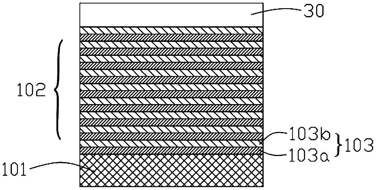
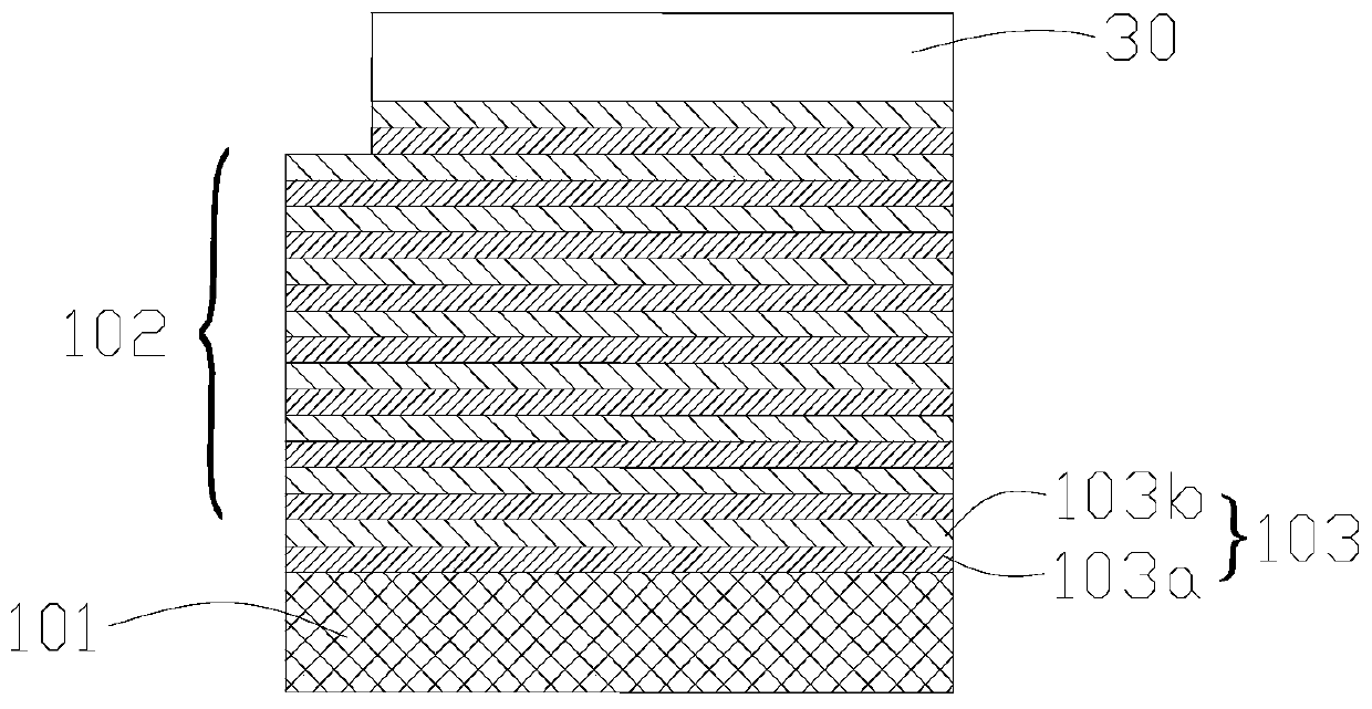
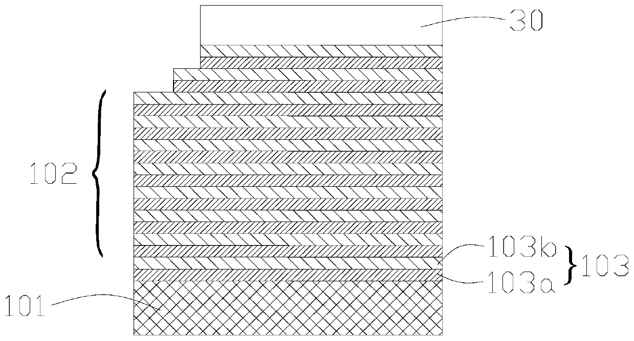
[0049] Before describing the specific implementation of the present invention, the traditional method for preparing a three-dimensional memory is briefly introduced. The general process is as follows: Figure 1-Figure 5 As shown, a stacked structure 102 is formed on a substrate 101, the stacked structure 102 includes a plurality of ...


PUM


Abstract

The invention provides a preparation method of a semiconductor device, and the preparation method comprises the following steps: providing a substrate, forming N layers of steps at the end part of thesubstrate, and connecting the horizontal plane of one layer of step with the vertical plane of the adjacent layer of step to form a corner; forming a barrier layer on the top surface of the substrate; forming a protective layer covering the corner, the protective layer having a side portion covering the vertical surface and an extension portion extending in a direction away from the vertical surface, the extension portion covering a part of the horizontal surface; etching the substrate by taking the barrier layer and the protective layer as masks to form a new step; and after the extension part is removed, continuously etching the substrate along the barrier layer and the protective layer so as to form a new step again. The technical problems that due to the fact that the number of timesof exposure and etching is large, the preparation speed of the three-dimensional memory is low, and the preparation cost is increased are solved.

Description

technical field [0001] The invention belongs to the technical field of semiconductors, and in particular relates to a preparation method of a semiconductor device. Background technique [0002] Three-dimensional memory (NAND) is a better storage device than hard disk drives, and has the advantages of low power consumption and light weight. Among them, the three-dimensional (3D) structure of NAND memory is due to the three-dimensional arrangement of memory cells on the substrate However, it has high integration density and large storage capacity, so it has been widely used in electronic products. [0003] The preparation method of the traditional three-dimensional memory step structure is to etch multiple stacked pairs of the stacked structure layer by layer. The thickness of each etching is one stacked pair. As the stacked structure becomes higher and higher, the number of times of exposure and etching Also with the increase, the manufacturing speed of the three-dimensional...

Claims


Application Information

Patent Timeline
Patent Type & Authority Applications(China)
IPC IPC(8): H01L27/11524H01L27/11551H01L27/1157H01L27/11578
CPCH10B41/35H10B41/20H10B43/35H10B43/20
Inventor 王启光
Owner YANGTZE MEMORY TECH CO LTD
Why Eureka
Try Eureka