Supercharge Your Innovation With Domain-Expert AI Agents!

Front opening unified pod

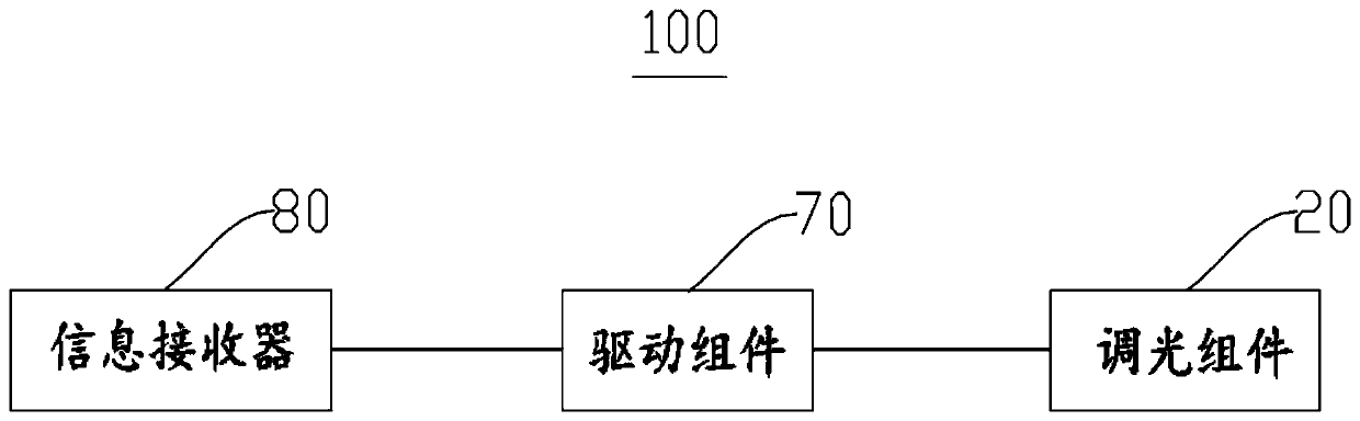
A wafer transfer box and dimming technology, which is applied to the manufacture of conveyor objects, electrical components, semiconductor/solid-state devices, etc., can solve problems affecting the electrical performance of wafers, and achieve the effect of ensuring electrical performance

Inactive Publication Date: 2020-01-21
YANGTZE MEMORY TECH CO LTD
View PDF5 Cites 0 Cited by
  • Summary
  • Abstract
  • Description
  • Claims
  • Application Information

AI Technical Summary

Problems solved by technology

[0003] In view of this, an embodiment of the present invention provides a FOUP, which solves the problem that the light in the prior art will pass through the visualization window of the FOUP to cause a photoelectric reaction on the wafers in the FOUP, thereby affecting the wafers. electrical performance issues

Method used


Image

  • Front opening unified pod
  • Front opening unified pod
  • Front opening unified pod

Examples


Embodiment Construction

[0030] Specific embodiments of the present invention will be described in more detail below with reference to the accompanying drawings. Although exemplary embodiments of the invention are shown in the drawings, it should be understood that the invention may be practiced in other ways than those described herein, and therefore, the invention is not limited by the following embodiments.

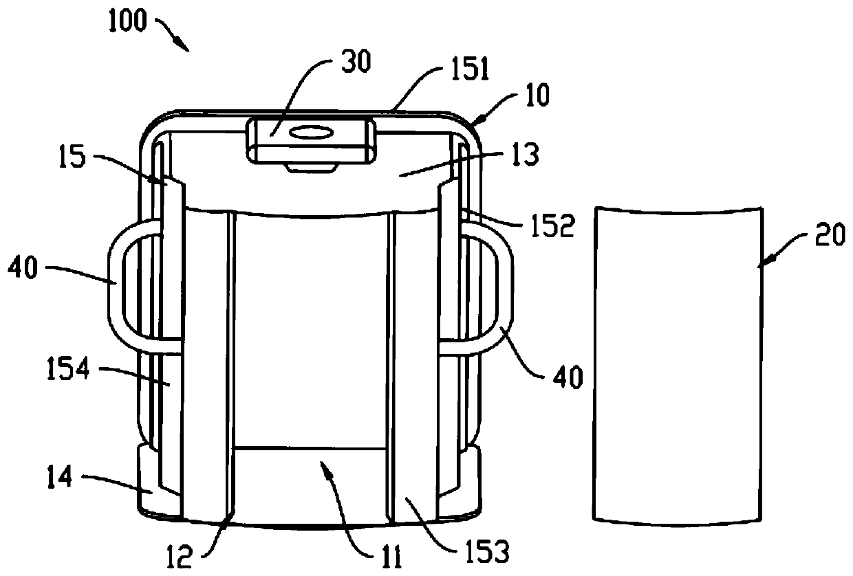
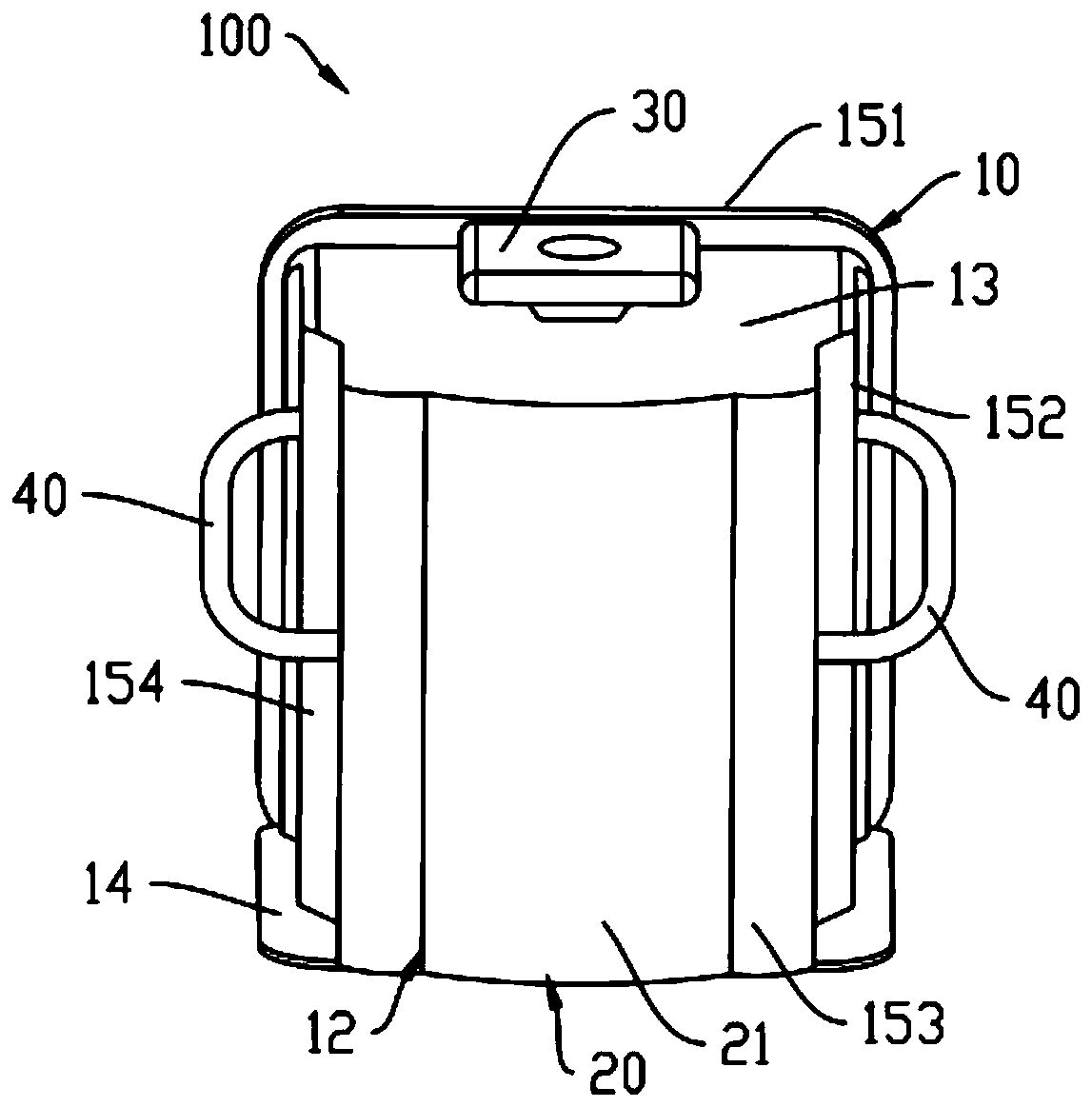
[0031] Front Opening Unified Pod (FOUP) is a container used to protect, transport, and store wafers in the semiconductor manufacturing process, and its accommodating space can accommodate multiple wafers. In the semiconductor manufacturing process, the wafer transfer box plays an extremely important role as a tool for temporary storage of wafers and wafer transfer between machines. The storage space of the FOUP is a closed space, and the internal environment is kept stable and clean, which can avoid direct contact between the wafer and the external environment, ensure the stability of the proc...


PUM


Abstract

The invention provides a front opening unified pod, which comprises a shell and a dimming assembly. The shell is provided with an accommodating space and a light transmitting part. The accommodating space is used for accommodating a wafer. The light transmitting part is used for transmitting external light into the accommodating space. The dimming assembly is arranged on the shell and covers the light transmitting part, and the dimming assembly can be switched between a light transmitting state and a light shielding state. When the dimming assembly is in the light transmitting state, externallight is allowed to be transmitted into the accommodating space. When the dimming assembly is in the light shielding state, the dimming assembly is used for shielding the external light. By using thefront opening unified pod of the invention, the problem that light can penetrate through a visual window of a front opening unified pod to enable a wafer in the front opening unified pod to generate photoelectric reaction and to affect the electrical performance of the wafer in the prior art is solved.

Description

technical field [0001] The invention relates to the technical field of electronic processing, in particular to a wafer transfer box. Background technique [0002] In the semiconductor manufacturing industry, a FOUP is a portable container for storing semiconductor wafers. During the wafer production process steps, due to various factors, wafers may be stored in the FOUP for a period of time. In the existing production process, light will pass through the visualization window of the FOUP to cause a photoelectric reaction on the wafer in the FOUP, thereby affecting the electrical properties of the wafer. Contents of the invention [0003] In view of this, an embodiment of the present invention provides a FOUP, which solves the problem that the light in the prior art will pass through the visualization window of the FOUP to cause a photoelectric reaction on the wafers in the FOUP, thereby affecting the wafers. electrical performance issues. [0004] An embodiment of the pr...

Claims


Application Information

Patent Timeline
IPC IPC(8): H01L21/673H01L21/677
CPCH01L21/673H01L21/6773
Inventor 马霏霏王庆高旭程仕峰陈金星
Owner YANGTZE MEMORY TECH CO LTD
Features
  • R&D
  • Intellectual Property
  • Life Sciences
  • Materials
  • Tech Scout
  • Unparalleled Data Quality
  • Higher Quality Content
  • 60% Fewer Hallucinations
Learn More