Blind hole processing method for multilayer printed board

A multi-layer printed board and processing method technology, which is applied in multi-layer circuit manufacturing, printed circuit manufacturing, printed circuit, etc., can solve the problem of increasing the manufacturing cost of printed boards, the inability to realize leaking pads, and the unusable finished printed boards And other issues

Active Publication Date: 2020-01-31
珠海杰赛科技有限公司 +1
View PDF8 Cites 0 Cited by
  • Summary
  • Abstract
  • Description
  • Claims
  • Application Information

AI Technical Summary

Problems solved by technology

Using the traditional process, the depth of the processed blind hole is not accurate, and after processing, there will be an adhesive layer in the hole that cannot be processed, and the leakage of the pad in the hole cannot be realized, so that the probe of the component cannot be used normally when inserted into the blind hole. Therefore, the traditional process method cannot process the part of the blind hole used to insert the component probe. The industry basically communicates with the designer and re-modifies the wiring design to meet the needs of installing the component probe. However, this method has the following disadvantages: Due to graphics limitations, when the ...

Method used


Image

  • Blind hole processing method for multilayer printed board
  • Blind hole processing method for multilayer printed board
  • Blind hole processing method for multilayer printed board

Examples


Embodiment Construction

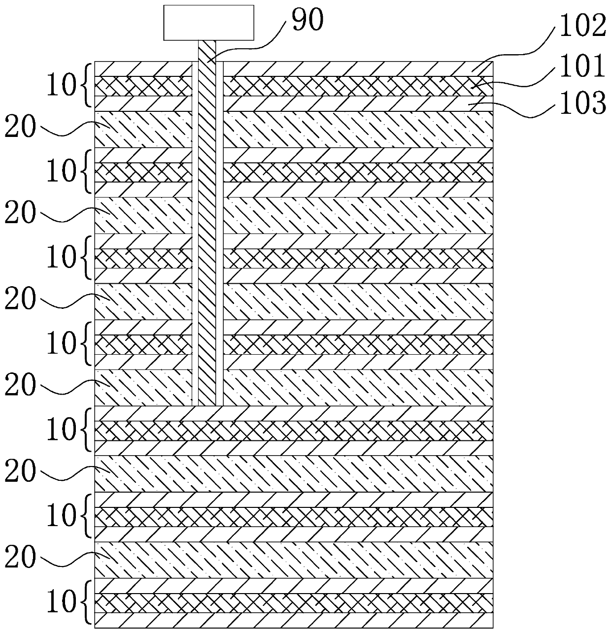
[0026] see figure 1 , in a blind hole processing method of a multilayer printed board of the present invention, the multilayer printed board includes an N+M layer core board 10, which is formed by laminating N+M layer core boards 10, wherein two adjacent layers There are prepregs 20 between the core boards, and the prepregs have a total of N+M-1 layers, that is, the multilayer printed board follows the first layer of core board, the first layer of prepreg, the second layer of core board, the second layer of prepreg... N-1 layer core board, N-1 layer prepreg, N layer core board... N+M-1 layer core board, N+M-1 layer prepreg, N+M layer core board arrangement order pressing The core board 10 includes a base material layer 101 and a first copper foil 102 and a second copper foil 103 respectively arranged on the upper and lower surfaces of the base material layer. When the probe 90 of the component is inserted into the blind hole 60, it needs to be The core board is inserted into ...


PUM


Abstract

The invention relates to the technical field of circuit board manufacturing, and discloses a blind hole processing method of a multi-layer printed board. The blind hole processing method comprises thefollowing steps: S1, processing process edge; S2, windowing of PP sheet; S3, hollowing out the PP sheet; S4, pressing in the early stage; S5, first back drilling; S6, pressing all chips; S7, second back drilling; and S8, obtaining the finished product. The setting of notches and windows in the steps S1 and S2 of the processing method can ensure that the first copper foil on the upper surface of the Nth layer core board at the notches is exposed and the pressing feet of the drilling machine can be pressed on the first copper foil of the Nth core plate after pressing of the core plate. Therefore, when the drill bit contacts the first copper foil on the upper surface of the Nth layer core plate, the press feet of the drilling machine and the drilling bit form a circuit to generate current and the drill bit stops drilling. Compared with the method of pressing the presser feet of the drilling machine on the first copper foil on the upper surface of the first layer core plate, the drillingdepth can be accurately controlled to ensure that the first copper foil on the upper surface of the Nth layer core plate is just drilled without drilling through the copper foil, thus ensuring the accuracy of the drilling depth and greatly improving the success rate of processing.

Description

technical field [0001] The invention relates to the technical field of circuit board manufacturing, in particular to a blind hole processing method of a multilayer printed board. Background technique [0002] Processing multi-layer interconnected printed boards with blind holes is one of the common printed board designs. At present, most of them are used in aerospace, military industry, and medical treatment. Some blind holes are used to insert component probes, such as figure 1 , the bottom of the probe needs to be attached to the printed board pad, that is, it needs to be attached to the copper surface leaking from the bottom of the hole, such as figure 1 . Using the traditional process, the depth of the processed blind hole is not accurate, and after processing, there will be an adhesive layer in the hole that cannot be processed, and the leakage of the pad in the hole cannot be realized, so that the probe of the component cannot be used normally when inserted into the b...

Claims


Application Information

Patent Timeline
IPC IPC(8): H05K3/42H05K3/46
CPCH05K3/421H05K3/4611H05K2201/09518H05K2203/0207
Inventor 房鹏博刘斌斌荀宗献赵丕然
Owner 珠海杰赛科技有限公司
Why Eureka
Try Eureka