Optical multilayer film, and optical component and display device comprising same
A technology of optical multilayer film and optical components, applied in optical elements, optics, nonlinear optics, etc., can solve problems such as low durability and reduced degree of polarization
- Summary
- Abstract
- Description
- Claims
- Application Information
AI Technical Summary
Problems solved by technology
Method used
Image

Examples
Embodiment 1
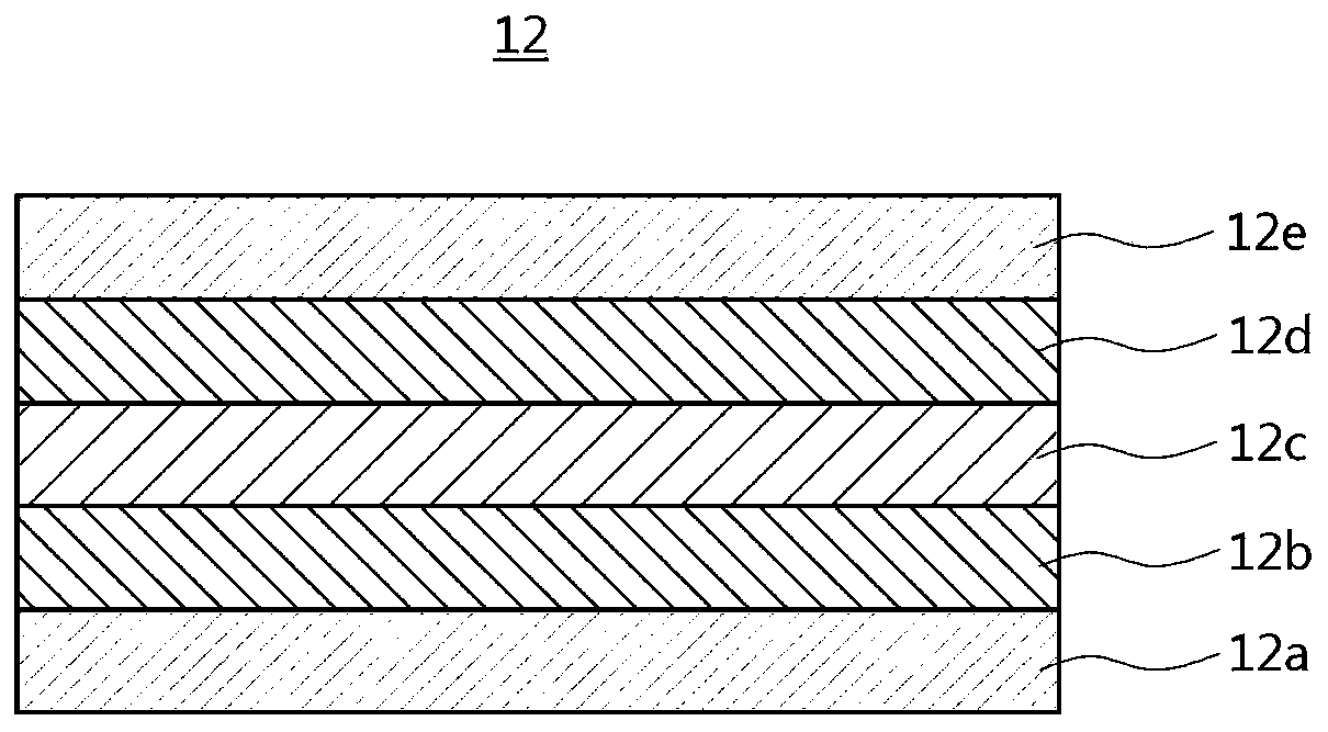
[0216] Embodiment 1: the making of optical multilayer film
[0217] Step (1) formation of substrate layer
[0218] Extrude polyethylene terephthalate resin (SKC company) through an extruder at about 280°C, and cast it through casting rolls at about 30°C to make unstretched sheets (sheet ). After preheating the unstretched sheet under the temperature conditions in Table 1 below, stretching was performed in the machine direction (MD) and tenter direction (TD) at a temperature of 125° C. according to the stretching ratios shown in Table 1. Thereafter, the stretched board was thermally cured for about 30 seconds at the temperature in Table 1 below to form a substrate layer.
[0219] Step (2) formation of undercoat
[0220] In the process of forming the base material layer, an undercoat layer is formed on the base material layer after stretching in the machine direction (MD) and before stretching in the tenter direction (TD). In this case, the base layer is formed by applying a...
experiment example 1
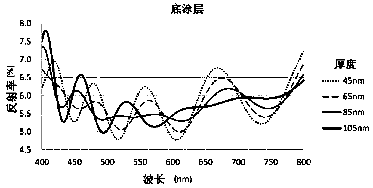
[0231] Experimental example 1: Measurement of reflectivity
[0232] The reflectance of the optical multilayer film produced in Example 1 above was measured.
[0233] After attaching a black tape on glass with little light absorption and attaching an optical multilayer film sample thereon, the reflectance was measured in a wavelength range of 400 nm to 800 nm using a spectrophotometer (U-4100, Hitachi).
[0234] Additionally, the same procedure as in Example 1 above was repeated, and the thickness of any layer was changed as shown below to produce individual optical multilayer films.
[0235] Specifically, after producing various optical multilayer films under the conditions of (a) to (d) below and measuring each reflectance, they are shown in Figure 3a to Figure 3d .
[0236] (a) changing the thickness of the undercoat layer from 45nm to 105nm;
[0237] (b) changing the thickness of the hard coat layer from 0.5 μm to 3.5 μm;
[0238] (c) changing the thickness of the firs...
experiment example 2
[0241] Experimental example 2: Evaluation of base material layer
[0242] Repeat the step (1) of the above-mentioned embodiment 1, and the specific production process conditions are as follows to prepare the polyester base material layer.
[0243] Table 2
[0244]
[0245] The following experiments were carried out on the above six substrate layer samples.
[0246] (1) Refractive index and in-plane retardation
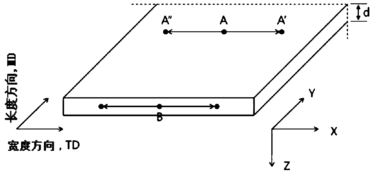
[0247] Refractive index ((nx+ny) / 2), in-plane retardation (Ro), thickness direction retardation (Rth), and in-plane retardation within effective width (|ΔRo| / |Δx|) were measured for the samples.
[0248] First, the orientation axis direction of the sample is obtained using two polarizing plates, and the sample is cut out into a rectangle of 4 cm×2 cm so that the orientation axis directions are perpendicular to each other. In-plane retardation (Ro) and thickness direction retardation (Rth) were measured at the width center using a retardation measuring device (man...
PUM
| Property | Measurement | Unit |
|---|---|---|
| thickness | aaaaa | aaaaa |
| thickness | aaaaa | aaaaa |
| thickness | aaaaa | aaaaa |
Abstract
Description
Claims
Application Information
 - R&D Engineer
- R&D Manager
- IP Professional
- Industry Leading Data Capabilities
- Powerful AI technology
- Patent DNA Extraction
Browse by: Latest US Patents, China's latest patents, Technical Efficacy Thesaurus, Application Domain, Technology Topic.
© 2024 PatSnap. All rights reserved.Legal|Privacy policy|Modern Slavery Act Transparency Statement|Sitemap