Multi-chip packaging protective silicone rubber tooling

A multi-chip packaging, silicone rubber technology, applied in electrical components, semiconductor/solid-state device manufacturing, circuits, etc., can solve problems such as fixing in one place and not being able to carry out at any time, not being able to package multiple chips at the same time, and affecting the efficiency of packaging, etc. To achieve the effect of simple structure, precise and stable fixation, and convenient use

Inactive Publication Date: 2020-02-18
安徽国晶微电子有限公司
View PDF0 Cites 1 Cited by
  • Summary
  • Abstract
  • Description
  • Claims
  • Application Information

AI Technical Summary

Problems solved by technology

[0003] At present, the chip packaging protection silicone rubber technology or equipment is only for a single chip packaging, and multiple chips cannot be packaged at the same time, which affects the efficiency of packaging, and the existing packaging can only be fixed in one place and cannot be carried out at any time. If in an emergency Next, the chip needs to be packaged, and the chip needs to be taken to the packaging equipment, which is easy to cause damage to the chip

Method used


Image

  • Multi-chip packaging protective silicone rubber tooling
  • Multi-chip packaging protective silicone rubber tooling
  • Multi-chip packaging protective silicone rubber tooling

Examples


Embodiment Construction

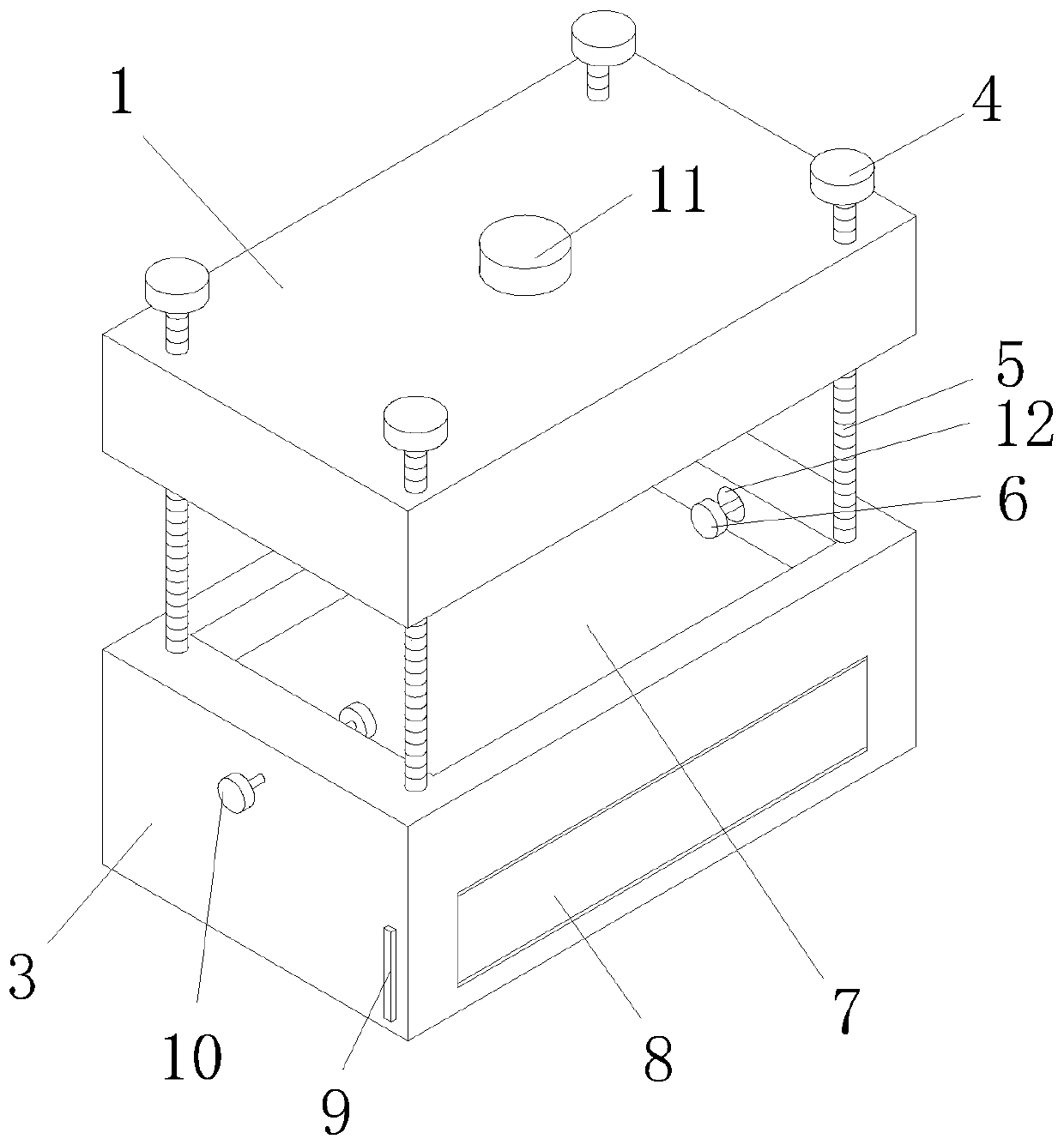
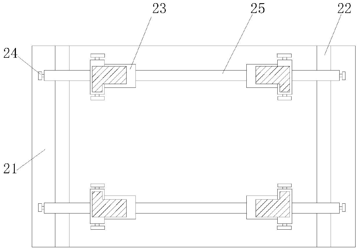
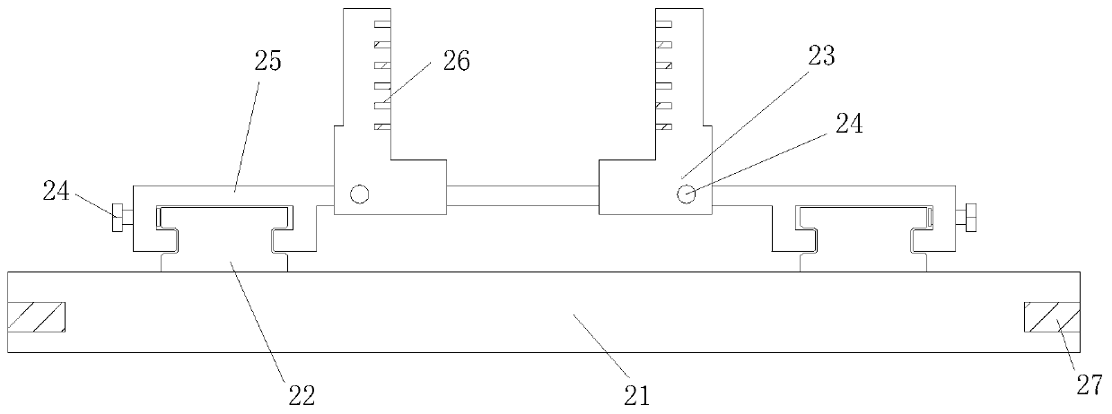
[0022] The present invention is described in further detail now in conjunction with accompanying drawing. These drawings are all simplified schematic diagrams, which only illustrate the basic structure of the present invention in a schematic manner, so they only show the configurations related to the present invention.

[0023] Examples of the described embodiments are shown in the drawings, wherein like or similar reference numerals designate like or similar elements or elements having the same or similar functions throughout. The embodiments described below by referring to the figures are exemplary and are intended to explain the present invention and should not be construed as limiting the present invention.

[0024] In describing the present invention, it should be understood that the terms "center", "longitudinal", "transverse", "length", "width", "thickness", "upper", "lower", "front", " Back", "Left", "Right", "Vertical", "Horizontal", "Top", "Bottom", "Inner", "Outer"...


PUM


Abstract

The invention discloses a multi-chip packaging protective silicone rubber tooling which comprises an upper mold device, a lower mold device and a chip placing device. The upper mold device and the lower mold device are connected through a screw rod, and a first placing groove for placing the chip placing device is arranged at the center. The screw rod is used for closing the upper mold device andthe lower mold device. The chip placing device comprises a table plate. Two longitudinal slide rails are arranged in parallel on the table plate. Two transverse guide rails are slidably arranged on the longitudinal slide rails. Two slide bases are respectively slidably arranged on the two transverse guide rails. Chip clamp grooves for placing chips are arranged on the corresponding side surfaces of the four slide bases. The tooling has a simple structure and is convenient to use and realizes simultaneous accurate positioning and clamping of a plurality of chips, and the cavity formed by the upper mold device and the lower mold device becomes a reserved space for pouring silicone rubber so as to meet the requirement of simultaneous silicone rubber packaging of a plurality of chips.

Description

technical field [0001] The invention relates to the technical field of chip packaging, in particular to tooling for multi-chip packaging protective silicone rubber. Background technique [0002] The chip is a precision electronic product. Impurities and water vapor in the external environment will corrode the precision circuit on the chip, which will cause damage to the chip. The protective silicon rubber around the chip can effectively prevent damage to the chip from the external environment. Chip packaging Technology is a process technology that wraps the chip to avoid contact between the chip and the outside world and prevent damage to the chip from the outside world. Impurities and bad gases in the air, and even water vapor will corrode the precision circuits on the chip, resulting in a decrease in electrical performance. Different packaging technologies differ greatly in terms of manufacturing processes and processes, and packaging also plays a vital role in the perfor...

Claims


Application Information

Patent Timeline
IPC IPC(8): H01L21/67H01L21/687
CPCH01L21/67121H01L21/68721
Inventor 范初阳阮怀其
Owner 安徽国晶微电子有限公司
Why Eureka
Try Eureka