Low-voltage stress ZVS high-gain Boost converter
A high-gain, low-voltage technology, applied in the electrical field, can solve the problems of aggravated electromagnetic interference, increased voltage stress of switching devices, and high voltage stress of switching tubes and diodes, and achieves the effect of reducing system loss and system cost.
- Summary
- Abstract
- Description
- Claims
- Application Information
AI Technical Summary
Problems solved by technology
Method used
Image
Examples
Embodiment Construction
[0026] The following will clearly and completely describe the technical solutions in the embodiments of the present invention in conjunction with the accompanying drawings in the embodiments of the present invention. Obviously, the described embodiments are only some of the embodiments of the present invention, not all of them. Based on the embodiments of the present invention, all other embodiments obtained by persons of ordinary skill in the art without making creative efforts belong to the protection scope of the present invention.
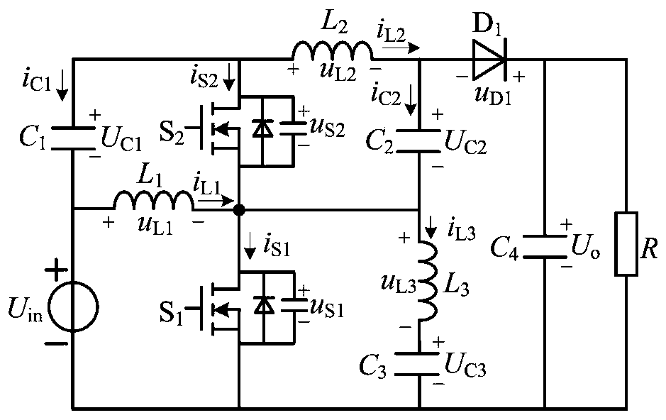
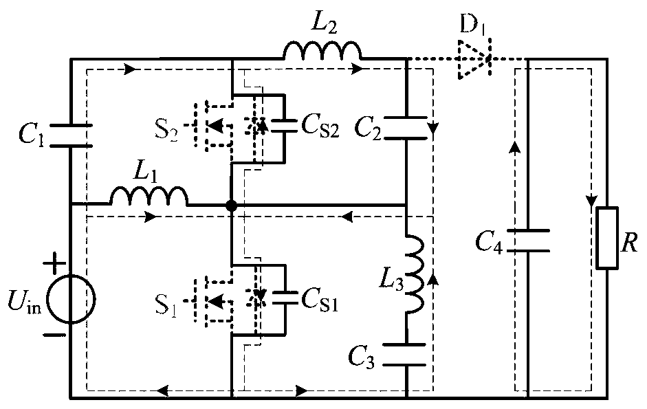
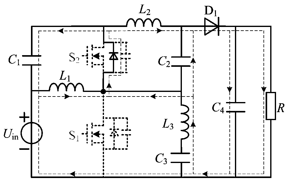
[0027] Please refer to figure 1 , figure 1 The schematic diagram of the circuit structure of the low-voltage stress ZVS high-gain Boost converter provided by the embodiment of the present application (in the figure, an N-channel MOS transistor is used as the switch tube, and the capacitors are all polarized capacitors), including the first switch tube S 1 , the second switch tube S 2 , Diode D 1 , the first inductance L 1 , the second induc...
PUM
 Abstract
Description
Claims
Application Information


