

Method for automatically creating via hole in copper sheet of PCB
An automatic creation and via technology, which is applied in the direction of instruments, electrical digital data processing, electrical components, etc., can solve the problems of uneven drilling and low efficiency, so as to improve efficiency and signal integrity, improve work efficiency, and alleviate The effect of current pressure
- Summary
- Abstract
- Description
- Claims
- Application Information
AI Technical Summary
Problems solved by technology
Method used
Image

Examples
Embodiment 1
[0028] This embodiment provides a method for automatically creating vias on the PCB copper skin, which is characterized in that: when the PCB is in the current window, when receiving external command information, it can automatically search and obtain the position information corresponding to the relevant command, And create and place ground vias as required in the instruction.
[0029] Further, the desired via hole can be arbitrarily selected in the current PCB, or a newly added one.
[0030] Further, the position information is automatically acquired on the current PCB network copper skin according to the currently set distances from vias to traces, pads and other network copper skin elements.
[0031] Further, the position information is calculated based on the ground copper laid on the current PCB as a reference.
[0032] Further, the creation of the location information of the ground vias includes the following steps:
[0033] S1. The file must be under the current PCB ...
Embodiment 2
[0039] This embodiment provides a method for automatically creating vias on the PCB copper skin, including the following steps:
[0040] Step 1. Under the current PCB interface, when receiving the command to automatically create ground vias, the distance information between all relevant elements on the current PCB and the ground copper network will be automatically obtained;
[0041] Step 2, the relevant elements of the PCB mainly refer to vias and traces, pads, and other network vias and copper skins; the automatically created vias need to keep a certain distance from these elements to avoid open and short circuits phenomenon, so it is necessary to manually set the distance between via holes and other elements and the distance between automatically placed hole arrays in the interface;
[0042] Step 3. After manually setting the distance from ground vias to traces, pads and related elements, the point will start to be created, and the program will automatically obtain the coor...
Embodiment 3
[0047]This embodiment provides a method for automatically creating vias on the copper skin of the PCB consistent with Embodiment 1, the difference is that the location information of the creation of ground vias includes the following steps:
[0048] Step 1: When receiving an external execution trigger, the program will check whether routkeepin / all is set in the outline of the board frame, and if so, proceed to the next step.
[0049] Step 2: The program will identify the size of the area where vias need to be placed according to the minimum coordinates x(0,0) and x(0,119), y(0,71) of the example board frame.
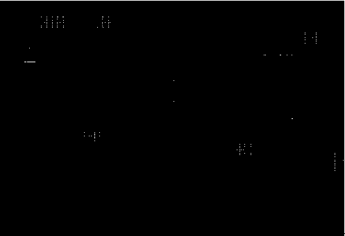
[0050] Step 3: The program will pop up as figure 2 In the user interface, you can select the size of the via hole to be placed in it, and set the distance between the via hole and the trace, the pad and the via copper skin of other networks. The default is 10mil; you also need to set the spacing of the via hole placement array. The program defaults to 100mil.
[0051]...
PUM
 Abstract
Description
Claims
Application Information