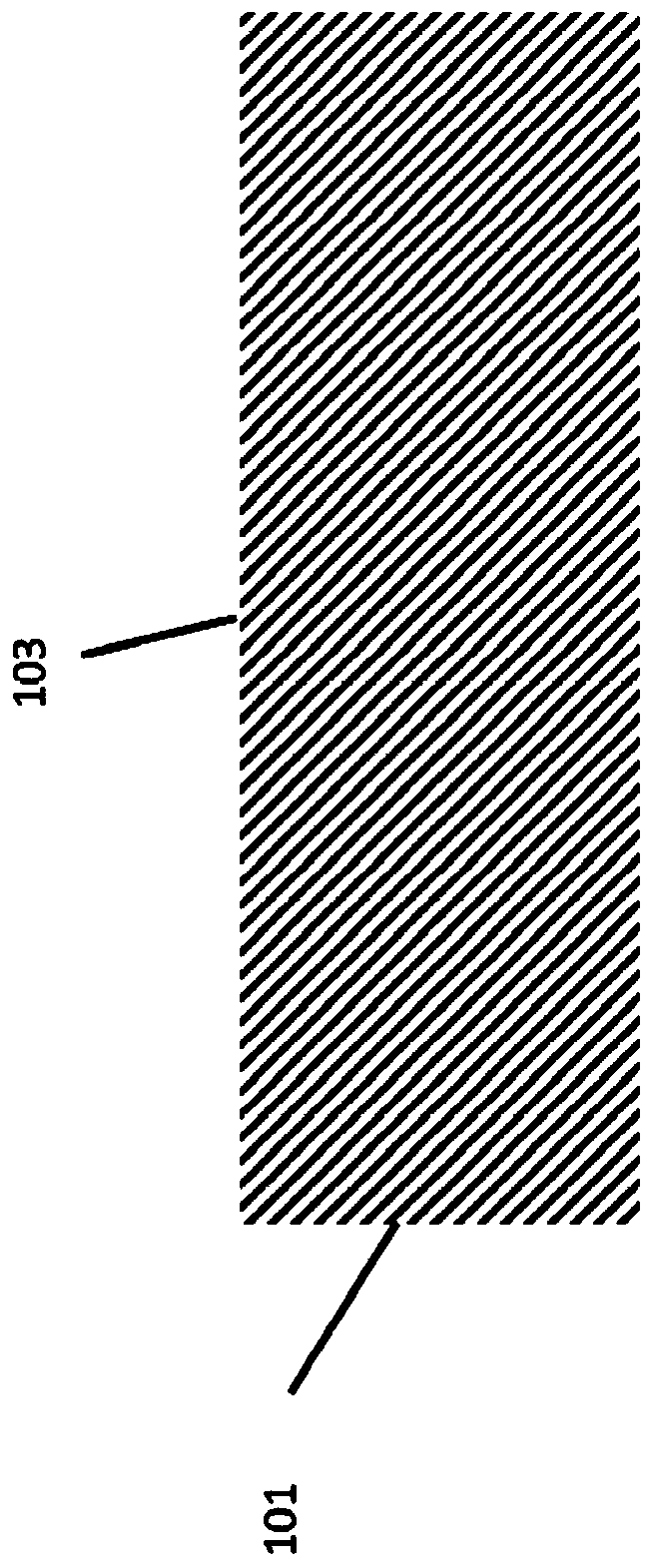
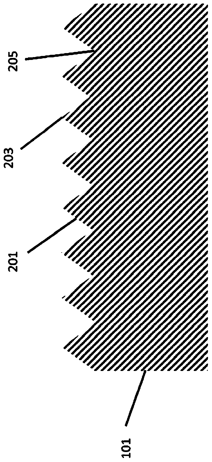
Stress relaxed buffer layer on textured silicon surface
A stress relaxation and non-flat technology, applied in the direction of semiconductor devices, electrical components, circuits, etc., can solve the problem of reducing the quality of the top epitaxial layer
- Summary
- Abstract
- Description
- Claims
- Application Information
AI Technical Summary
Problems solved by technology
Method used
Image

Examples
Embodiment Construction
[0026] In the following description, for purposes of explanation, numerous specific details are set forth in order to provide a thorough understanding of the exemplary embodiments. It is evident, however, that the example embodiments may be practiced without these specific details or with an equivalent arrangement. In other instances, well-known structures and devices are shown in block diagram form in order to avoid unnecessarily obscuring the illustrative embodiments. In addition, unless otherwise indicated, all numerical quantities, ratios, and numerical properties of constituents, reaction conditions, and the like used in the specification and claims should be understood to be understood by the term "about" All examples are modified.
[0027] The present disclosure solves the current problem of generating dislocation defects when growing semiconductor materials, such as stress relaxation buffer layers, on silicon wafers.
[0028] A method according to a disclosed embodim...
PUM
| Property | Measurement | Unit |
|---|---|---|
| depth | aaaaa | aaaaa |
Abstract
Description
Claims
Application Information
 - R&D
- Intellectual Property
- Life Sciences
- Materials
- Tech Scout
- Unparalleled Data Quality
- Higher Quality Content
- 60% Fewer Hallucinations
Browse by: Latest US Patents, China's latest patents, Technical Efficacy Thesaurus, Application Domain, Technology Topic, Popular Technical Reports.
© 2025 PatSnap. All rights reserved.Legal|Privacy policy|Modern Slavery Act Transparency Statement|Sitemap|About US| Contact US: help@patsnap.com