Method for forming COF circuit

A circuit and substrate technology, applied in the field of COF circuit forming, can solve the problems of poor pattern, slow production speed of exposure process, poor circuit, etc., and achieve the effect of shortening processing cycle, reducing short circuit defects and reducing equipment cost.

Inactive Publication Date: 2020-02-28
江苏上达半导体有限公司
View PDF5 Cites 1 Cited by
  • Summary
  • Abstract
  • Description
  • Claims
  • Application Information

AI Technical Summary

Problems solved by technology

[0004] ①The production speed of the exposure process is very slow, so in order to balance the production line, a large amount of equipment needs to be equipped here to meet the production capacity requirements, so the cost of equipment is very high;
[0005] ②If the energy of the exposure machine is unstable during the exposure process, it will cause poor exposure, and bad patterns will be obtained in the subsequent development, and the final circuit will also be bad;
[0006] ③If there are foreign objects in the production process, it will also cause defects in the exposure process, which will eventually lead to the appearance of a large number of defective products;
[0007] ④ Changes in process parameters during the development process will also cause poor development, which will eventually lead to poor open and short circuits in the product;
[0008] ⑤ During the development process, if the product has developer residue, it will also affect the subsequent circuit etching

Method used


Image

  • Method for forming COF circuit
  • Method for forming COF circuit
  • Method for forming COF circuit

Examples


Embodiment

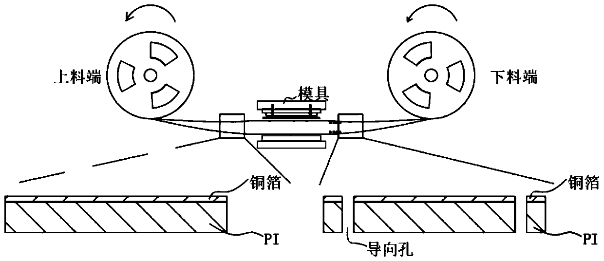
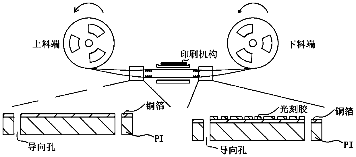
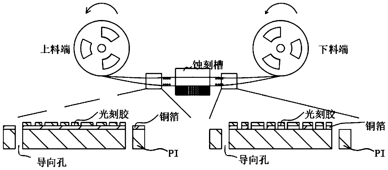
[0027] Such as Figure 1-4 As shown, the embodiment of the present invention provides a method for forming COF lines, which includes the following steps:

[0028] S1. Punching the base material and punching out the guide holes on both sides of the base material, which is convenient for the conveying operation of the later process;

[0029] S2, the punched product is printed with photoresist, and the required photoresist pattern is printed on the surface of the copper foil and cured;

[0030] S3. Perform etching on the product printed with photoresist patterns, and remove the copper that is not covered by the photoresist under the action of the etching solution;

[0031] S4. Fade the etched product, remove the photoresist pattern protected on the copper surface, and expose the circuit pattern;

[0032] S5. Follow-up processing of the product.

[0033] In the present invention, the circuit is formed by printing, and the work of the exposure and development process is omitted, thus reducin...


PUM


Abstract

The invention provides a method for forming a COF circuit and relates to the technical field of integrated circuits. The method for forming the COF circuit comprises steps that S1, a base material ispunched, and guide holes on two sides of the base material are punched; S2, photoresist printing of a punched product is performed, and a required photoresist pattern is printed on a surface of a copper foil and cured; S3, the product printed with the photoresist pattern is etched, and the copper which is not covered by the photoresist under the action of an etching solution is removed; and S4, afilm of the etched product is stripped, the photoresist pattern protected on the copper surface is removed, and the circuit pattern is exposed. The method is advantaged in that circuit forming is carried out in a printing manner, operations of exposure and development processes are omitted, so occurrence of bad short circuit conditions is reduced, cost of the exposure and development processes isgreatly saved, a product processing period can be shortened, and equipment cost is greatly reduced.

Description

Technical field [0001] The invention relates to the technical field of integrated circuits, and in particular to a method for forming COF lines. Background technique [0002] With the increasing portability and diversification of functions of electronic products, the requirements for integrated circuits are getting higher and higher. In order to meet these needs, the demand for COF packaging substrates is also increasing. The domestic COF industry is also rising. The COF processed by the RTR method is complicated in the process, and the tempo of each process varies greatly, especially the exposure process. The exposure process is an important part of the line forming process. In order to achieve the balance of the production line, it also requires a lot of equipment matching. the cost of. [0003] In the current COF production process, circuit formation is performed in accordance with the traditional exposure and development method, which has the following defects: [0004] ① The p...

Claims


Application Information

Patent Timeline
Patent Type & Authority Applications(China)
IPC IPC(8): H05K3/06
CPCH05K3/064H05K2203/0551
Inventor 徐世明王健孙彬沈洪李晓华
Owner 江苏上达半导体有限公司
Why Eureka
Try Eureka