

Test method, equipment and computer storage medium for asic chip wafer
An ASIC chip and test method technology, applied in the field of electronics, can solve the problems of low test efficiency of batch ASIC chips, and achieve the effects of reducing test land and test labor costs, improving productivity per unit time, and reducing test time.
- Summary
- Abstract
- Description
- Claims
- Application Information
AI Technical Summary
Problems solved by technology
Method used
Image

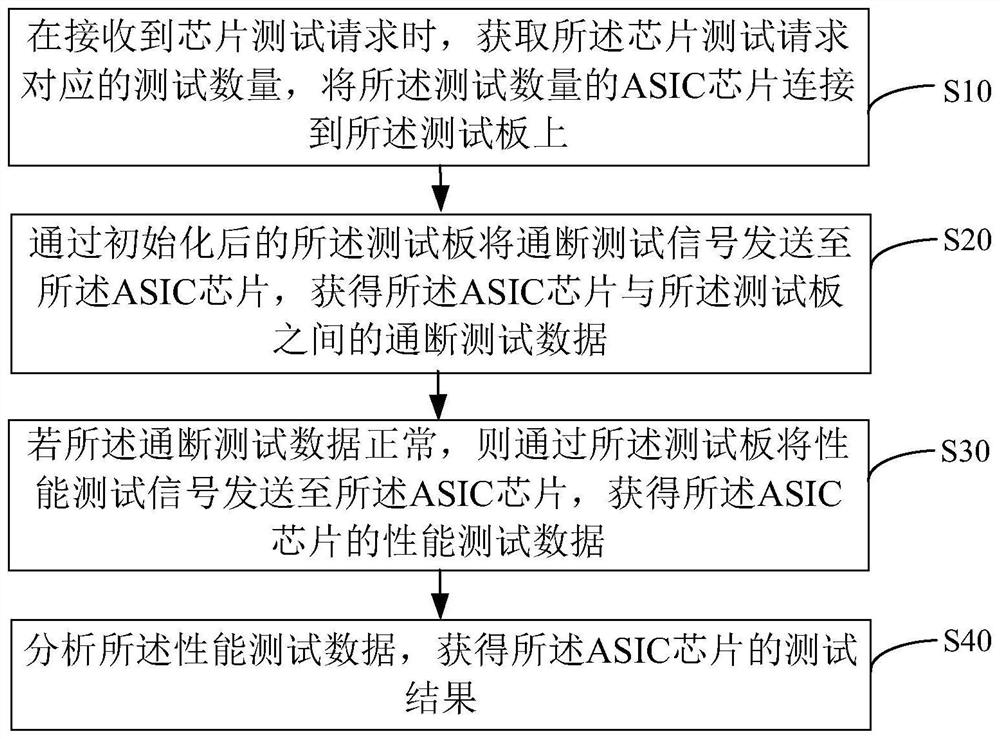
Examples
Embodiment Construction
[0047] It should be understood that the specific embodiments described here are only used to explain the present invention, not to limit the present invention.
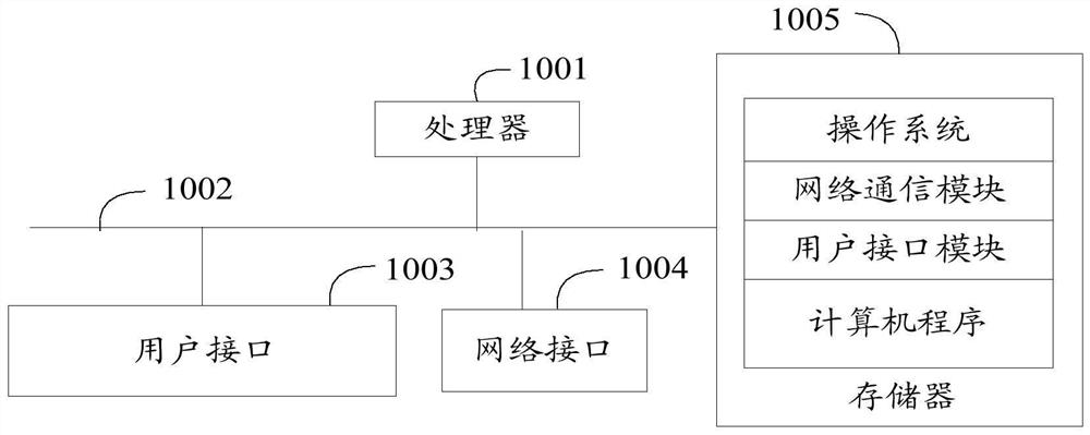
[0048] Such as figure 1 as shown, figure 1 It is the test equipment of the ASIC chip wafer of the hardware operating environment that the embodiment of the present invention scheme relates to (called the terminal again, wherein, the test equipment of the ASIC chip wafer can be made up of the test device of independent ASIC chip wafer, also can be It is formed by the combination of other devices and the testing device of ASIC chip wafer) Schematic diagram of the structure.
[0049]The terminal in the embodiment of the present invention can be a fixed terminal or a mobile terminal, such as an intelligent air conditioner with a networking function, an intelligent light, an intelligent power supply, an intelligent speaker, an automatic driving car, a PC (personal computer), a smart phone, a tablet computer , e-book read...
PUM
 Abstract
Description
Claims
Application Information