

Clamp for mounting a plurality of laser chips
A chip mounting and laser technology, applied in semiconductor/solid-state device manufacturing, electrical components, circuits, etc., can solve problems affecting the accuracy and quality of placement, inaccurate equipment positioning, and anti-soldering offset, etc., to improve accuracy and Quality, prevent reference position deviation, and facilitate clamping effect
- Summary
- Abstract
- Description
- Claims
- Application Information
AI Technical Summary
Problems solved by technology
Method used
Image

Examples
Embodiment 1
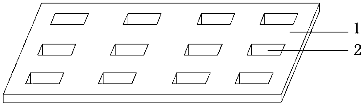
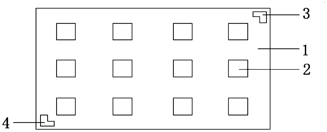
[0023] see figure 1 , 2 , a fixture for mounting multiple laser chips, the surface of the substrate 1 is provided with a through hole 2, and the upper right side of the top surface of the substrate 1 is provided with an optical positioning point a3, and the optical positioning point a3 is fixed on the substrate 1 by screws, and the substrate 1 There is an optical positioning point b4 on the lower right side of the top surface, and the optical positioning point b4 is fixed on the base plate 1 by screws. The point a3 and the optical positioning point b4 effectively prevent the offset of the reference position of the optical positioning point due to ink offset, thereby effectively improving the accuracy and quality of the placed part.
Embodiment 2
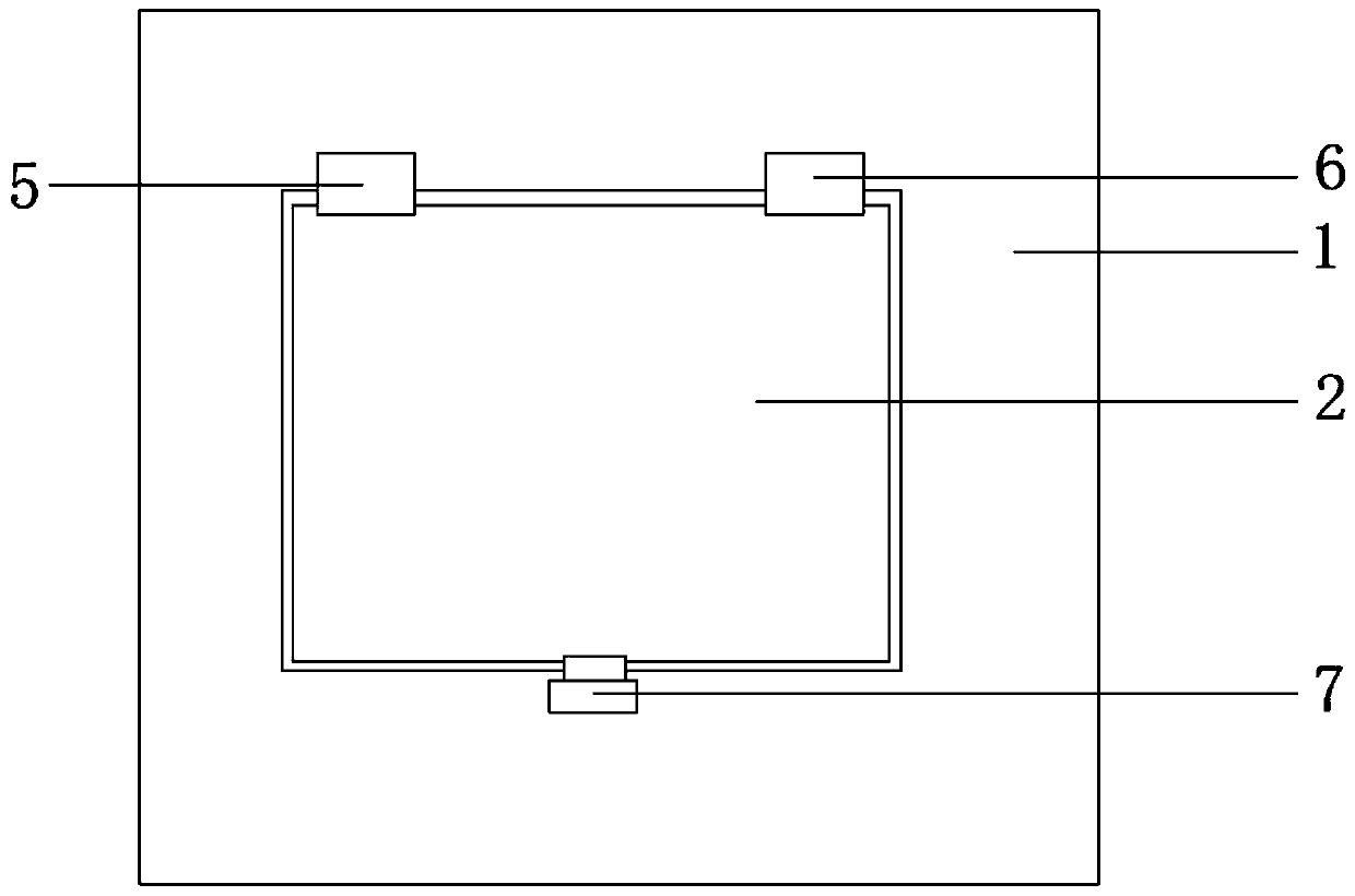
[0025] see image 3 , 4 , 5, a fixture for mounting multiple laser chips, a limit block a5 is provided on the upper left side of the through hole 2, the limit block a5 is fixed on the substrate 1 by screws, and a rubber layer is provided at the bottom of the limit block a5 9. The rubber layer 9 is made of antistatic rubber, and the right side of the rubber layer 9 is provided with a chamfer 8, and the rubber layer 9 is fixed on the limit block a5 by glue, and the limit block a5 is provided with a limit block b6 on the right side, and the limit block b6 is fixed on the substrate 1 by screws, a spring block 7 is arranged in the middle of the bottom of the through hole 2, and the spring block 7 is fixed on the substrate 1 by screws, and the limit block a5, the limit block b6 and the spring block 7 are all fixed on the substrate 1 The back of the spring block 7 is provided with a bump 10 above the inside, the bump 10 is fixed in the spring block 7 through a sleeve, the bump 10 ca...
PUM
 Abstract
Description
Claims
Application Information