
Chip pin missing detection method based on semi-supervised deep learning

A deep learning and detection method technology, applied in the field of computer vision and deep learning, can solve the problems of chip types, models, placement angle restrictions, difficult maintenance and use, and low detection accuracy, so as to reduce the difficulty of use and maintenance, Reduce the difficulty of maintenance and use, improve the effect of detection accuracy

Active Publication Date: 2020-03-27
深圳市海芯微迅半导体有限公司
View PDF10 Cites 9 Cited by
  • Summary
  • Abstract
  • Description
  • Claims
  • Application Information

AI Technical Summary

Problems solved by technology

The general detection method is template matching, but this method requires too high accuracy of thresholding segmentation, and a slight difference in the parameters of the light source and camera may lead to the failure of the entire system
Such systems require frequent manual maintenance, regular calibration and parameter adjustment
Moreover, the template matching method is too targeted and can only detect a specific chip, and there are restrictions on the type, model, and placement angle of the chip.
For other types of chips, the detection accuracy is low
The chip has the characteristics of small size, large production volume, and a large number of chips to be tested. The current chip detection technology detects the chips one by one, which is easy to miss, and the detection process is cumbersome and the detection efficiency is low.
[0004] Therefore, the existing chip pin missing detection technology has the problems of excessive specificity, difficulty in maintenance and use, low detection accuracy, and low detection efficiency.

Method used


Image

  • Chip pin missing detection method based on semi-supervised deep learning
  • Chip pin missing detection method based on semi-supervised deep learning
  • Chip pin missing detection method based on semi-supervised deep learning

Examples


Embodiment 1

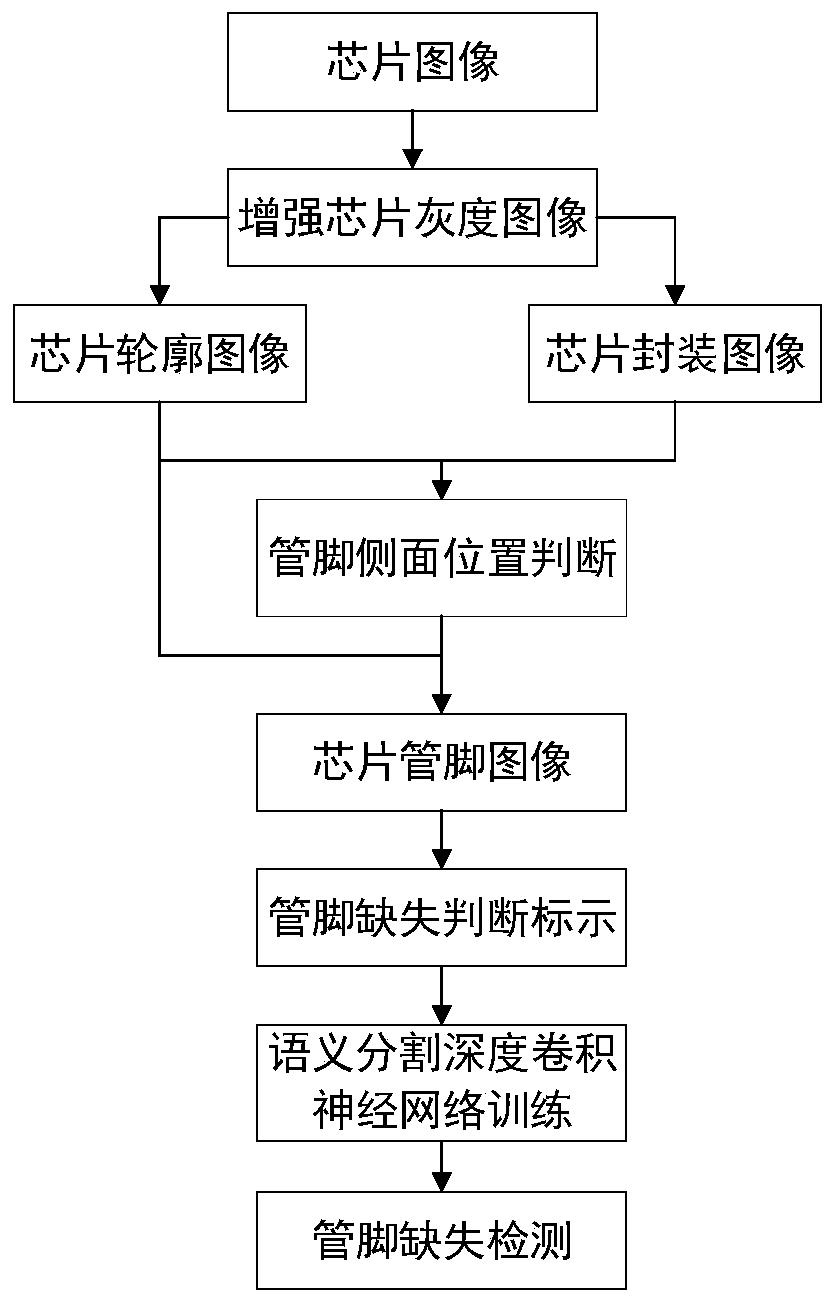
[0037] A chip pin missing detection method based on semi-supervised deep learning, the method includes:

[0038] In step 1, the chip image collected by the camera is preprocessed to obtain an enhanced grayscale image of the chip.

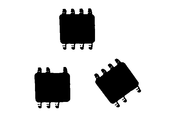
[0039] One embodiment is to use a color area scan camera to capture images of the chip. The dark color of the chip packaging part is generally black or dark black, and the color of the chip pin part is generally metallic silver. chip image as figure 2 shown. The preprocessing includes: performing grayscale processing on the chip image, normalizing the grayscale processing result, and performing image enhancement on the normalized result to obtain an enhanced chip grayscale image.

[0040] First, the collected color chip image is processed to obtain the RGB data of the collected chip image. Using the dark channel prior method, take the minimum value for the corresponding position components of the three channels, and obtain the chip grayscale im...


PUM


Abstract

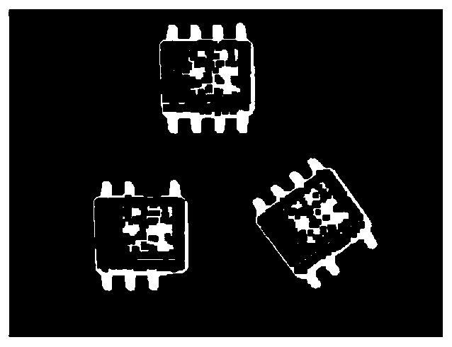
The invention discloses a chip pin missing detection method based on semi-supervised deep learning. The method comprises the following steps: preprocessing a chip image to obtain an enhanced chip grayscale image; carrying out edge detection, thresholding and morphological filtering processing on the enhanced chip grayscale image to obtain a chip contour image and a chip packaging image; carrying out connected domain detection on the chip contour image and the chip packaging image, and obtaining the side face, with the pins, of the chip through judgment; generating a packaging mask image according to the judgment result of the side surface, with the pins, of the chip, and multiplying the packaging mask image by the chip contour image in a point-to-point manner to obtain a chip pin image; carrying out pin missing judgment and marking on the chip pin image; training a semantic segmentation deep convolutional neural network according to the marking result; and utilizing the trained semantic segmentation deep convolutional neural network to carry out pin missing detection on the to-be-detected chip image. According to the invention, chip pin missing detection can be realized in a chip quality detection scene, and the detection efficiency and precision are improved.

Description

technical field [0001] The invention relates to the technical fields of computer vision and deep learning, in particular to a chip pin missing detection method based on semi-supervised deep learning. Background technique [0002] In today's society, the status of circuit chips is very important. The scope of application is getting wider and wider, and the number of uses has also increased sharply. After the chips are produced, they need to be packaged with cores, peripheral circuits, and pins. The number of chips produced If there are too many, there will inevitably be many defective defects, and the missing pins will have a great impact on chip production, and have a great impact on the quality of the product and the reputation of the manufacturer. Because of the huge quantity, the cost of manual inspection will be very high, and intelligent inspection is an important way to reduce costs. [0003] In general, chips with the same function will be derived into many models. ...

Claims


Application Information

Patent Timeline
Patent Type & Authority Applications(China)
IPC IPC(8): G06T7/00G06N3/04G06N3/08G06T7/13G06T7/136G06T7/187
CPCG06T7/0006G06T7/13G06T7/136G06T7/187G06N3/08G06T2207/20036G06T2207/20024G06N3/045
Inventor 窦宝恒李坤彬
Owner 深圳市海芯微迅半导体有限公司
Learn More