
Eureka
For R&D, Eureka makes reading and utilizing patents & technical documents easy.
Eureka AIR
Designed for self-driven R&D workflows. Generate viable solutions, solve complex R&D challenges, empower your innovation with AI.

Eureka Materials
Designed for material experts only. Revolutionize your material R&D, from search, analyze, to developing new materials.

TechResearch
Generate reliable direction feasibility study reports for your R&D in just a few steps.

TechSeek
Discover and master advanced knowledge NOW. Basics, ideas, possibilities, all at once.

TechMind
As an expert in R&D Theories, TechMind can generates customized viable solutions instantly.

TechRisk
Analyze your overall solution with one click, know your potential R&D risks in advance.

TechMonitor
Get weekly tech updates, stay abreast of the latest tech innovations and key insights.
Photodiode and preparation method thereof, display substrate and display device
A technology of photodiodes and display substrates, applied in radiation control devices, circuits, electrical components, etc., can solve problems such as unfavorable full-screen display, complex light sensor structure, and affecting the display effect of the display screen
- Summary
- Abstract
- Description
- Claims
- Application Information
AI Technical Summary
Problems solved by technology
Method used
Image

Examples
Embodiment 1
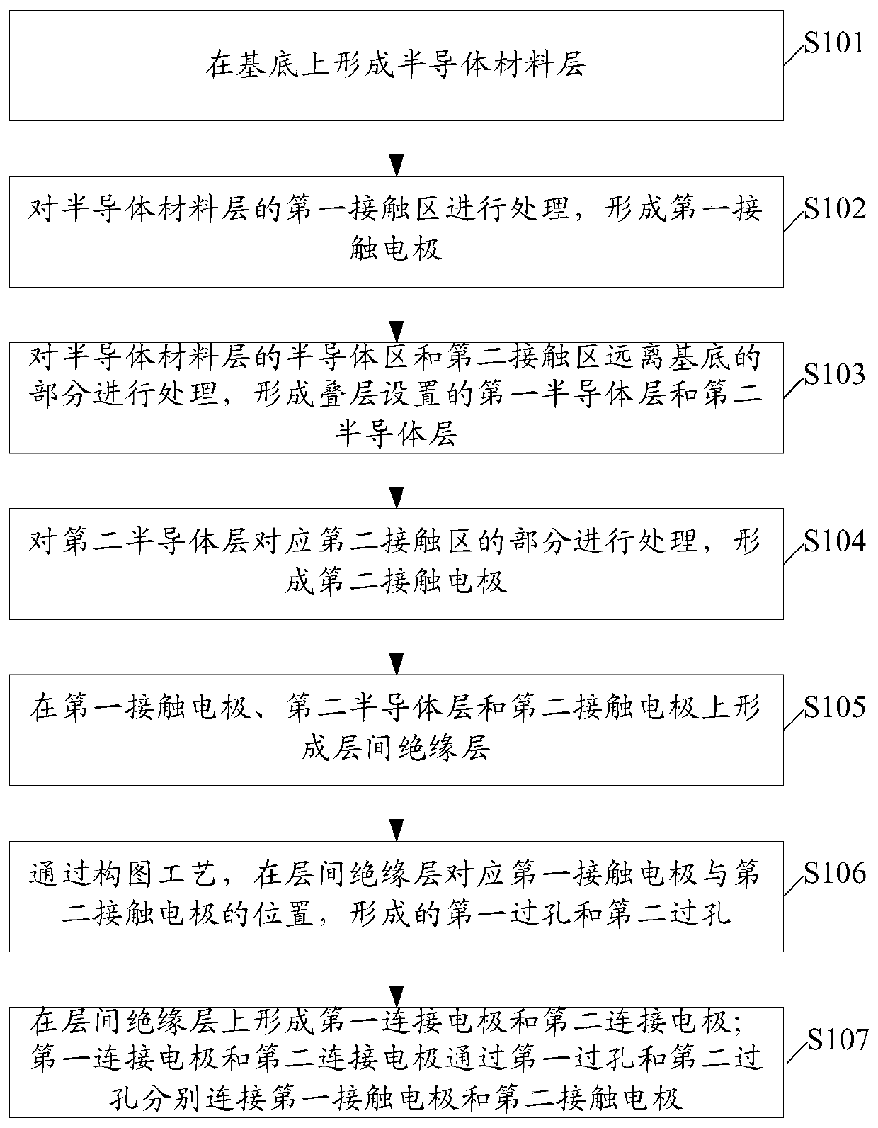
[0047] figure 1 A schematic flow diagram of a method for preparing a photodiode provided by an embodiment of the present invention, as figure 1 Shown, the preparation method of this photodiode comprises the steps:
[0048] S101, forming a semiconductor material layer on a substrate.
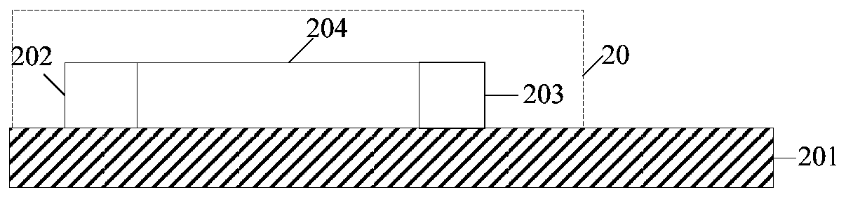
[0049] Such as figure 2 As shown, a layer of semiconductor material layer 20 can be formed on a substrate 201 by using a semiconductor material. The semiconductor material layer 20 includes: a first contact region 202, a second contact region 203, and a The semiconductor region 204 between the contact regions 203 . It can be understood that the semiconductor material may be a P-type semiconductor or an N-type semiconductor. In the embodiment of the invention, the semiconductor material is a P-type semiconductor as an example for illustration.
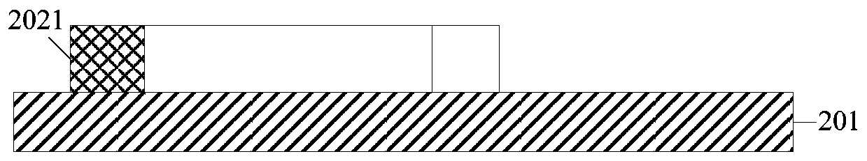
[0050] S102, processing the first contact region of the semiconductor material layer to form a first contact electrode.
[0051] Such as image 3 ...
Embodiment 2
[0072] Based on the same inventive concept, an embodiment of the present invention provides a photodiode, and the structure of the photodiode can be as follows Figure 8 As shown, the photodiode includes: a substrate 201, a first semiconductor layer 2041, a second semiconductor layer 2042, a first contact electrode 2021, a second contact electrode 2031, an interlayer insulating layer 205, a first via hole 206, a second via hole hole 207 , first connection electrode 208 and second connection electrode 209 .
[0073] The first semiconductor layer 2041 is located on the substrate 201; the first contact electrode 2021 is located at one end of the first semiconductor layer 2041; the second semiconductor layer 2042 is located on the first semiconductor layer 2041; the second contact electrode 2031 is located on the second semiconductor layer 2042 away from the first semiconductor layer One end of a contact electrode 2021; the interlayer insulating layer 205 is located on the first c...
Embodiment 3
[0076] An embodiment of the present invention provides a display substrate, and the display substrate includes the photodiode provided in the above embodiment. The display substrate has a display area and a non-display area. The photodiode is located in the non-display area of the display substrate. While sensing ambient light, the photodiode can avoid blocking the display area of the display substrate and affecting the display effect.
[0077] Optionally, the display substrate further includes: a pixel unit located in the display area of the display substrate, and a first power supply terminal and a second power supply terminal connected to the pixel unit; the first power supply terminal is connected to the first connection electrode; the second power supply terminal Connect to the second connection electrode.
[0078] It should be noted that, the first power supply terminal and the second power supply terminal can provide driving current for the display device in the p...
PUM
 Abstract
Description
Claims
Application Information
 - R&D Engineer
- R&D Manager
- IP Professional
- Industry Leading Data Capabilities
- Powerful AI technology
- Patent DNA Extraction
Browse by: Latest US Patents, China's latest patents, Technical Efficacy Thesaurus, Application Domain, Technology Topic, Popular Technical Reports.
© 2024 PatSnap. All rights reserved.Legal|Privacy policy|Modern Slavery Act Transparency Statement|Sitemap|About US| Contact US: help@patsnap.com