OLED display panel and preparation method thereof

A display panel and display area technology, which is applied in semiconductor/solid-state device manufacturing, electrical components, electric solid-state devices, etc., can solve the problems of reducing the display quality of WOLED display panels, improve electrical light leakage, improve luminous uniformity, and avoid crosstalk Effect

Inactive Publication Date: 2020-04-10
SHENZHEN CHINA STAR OPTOELECTRONICS SEMICON DISPLAY TECH CO LTD
View PDF7 Cites 19 Cited by
  • Summary
  • Abstract
  • Description
  • Claims
  • Application Information

AI Technical Summary

Problems solved by technology

This electrical light leakage phenomenon is particularly obvious in full-color WOLED display panels, thereby reducing the display quality of WOLED display panels

Method used


Image

  • OLED display panel and preparation method thereof
  • OLED display panel and preparation method thereof
  • OLED display panel and preparation method thereof

Examples


Embodiment Construction

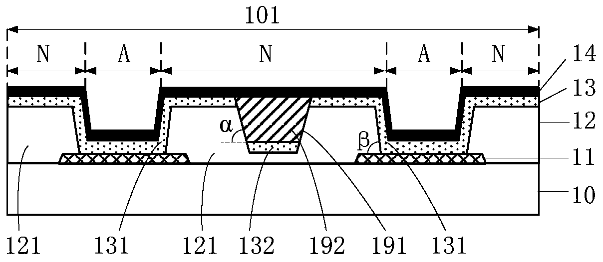
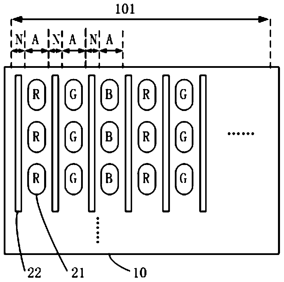
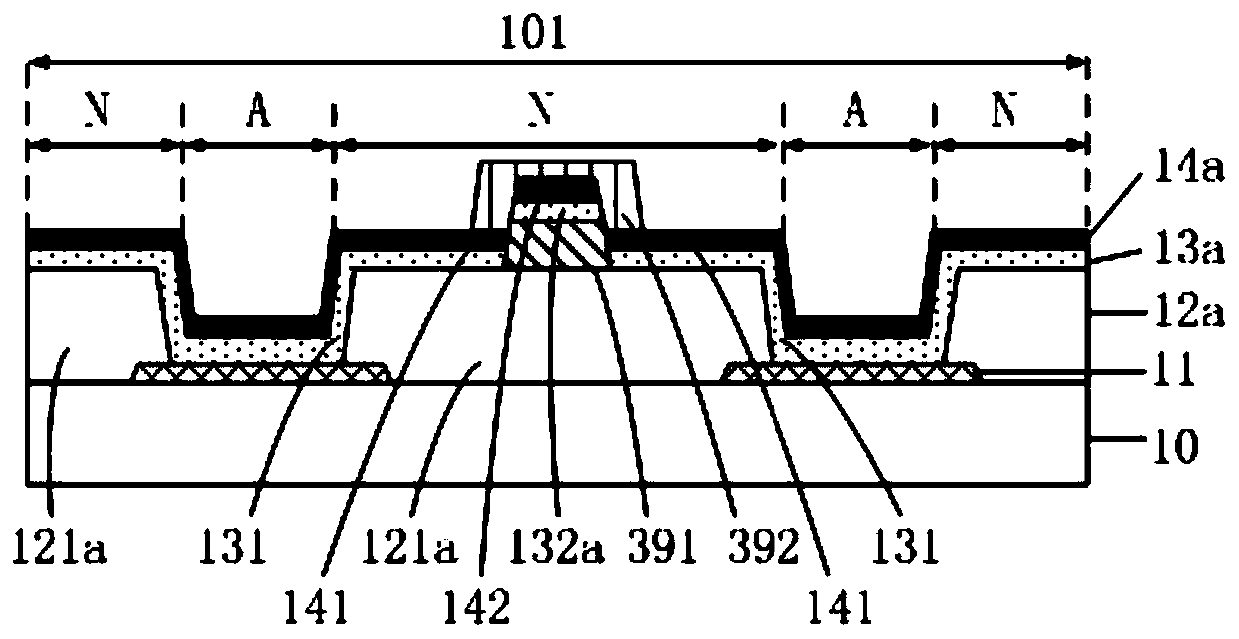
[0016] Embodiments of the present invention are described in detail below, examples of which are shown in the drawings, wherein the same or similar reference numerals denote the same or similar components or components having the same or similar functions throughout. The terms "first", "second", "third", etc. (if any) in the description and claims of the present invention and the drawings are used to distinguish similar objects and not necessarily to describe a specific order or sequence . It should be understood that the items so described are interchangeable under appropriate circumstances. Furthermore, the terms "comprising" and "having", as well as any variations thereof, are intended to cover a non-exclusive inclusion. The directional terms mentioned in the present invention, such as: up, down, left, right, front, back, inside, outside, side, etc., are only directions referring to the drawings. The embodiments described below with reference to the drawings and the direc...


PUM

PropertyMeasurementUnit
angleaaaaaaaaaa
angleaaaaaaaaaa
angleaaaaaaaaaa

Abstract

The invention discloses an OLED display panel and a preparation method thereof, and the method comprises the steps: blocking a light-emitting function layer of an OLED device in a non-light-emitting region between two adjacent columns of sub-pixels, so as to enable an electron not to transversely migrate in a hole injection layer and a charge generation layer to generate a leakage current; and ensuring a cathode layer to be in a whole-surface communication state in a light-emitting region corresponding to the sub-pixels and the non-light-emitting region between the sub-pixels, so that the pixels normally emit light.

Description

technical field [0001] The invention relates to the technical field of semiconductors, in particular to an OLED display panel and a preparation method thereof. Background technique [0002] Organic Light Emitting Diode (OLED for short) display devices use organic light-emitting materials to form a film by evaporation. When a current flows, these organic light-emitting materials will emit light, so there is no need for a backlight. By using a very thin organic material coating, the OLED display screen can be made lighter and thinner, and the viewing angle of the OLED display screen is larger, and can significantly save power. [0003] The core component of an OLED display device is an OLED display panel. The structure of an OLED display panel usually includes: a TFT array substrate and an anode sequentially fabricated on the TFT substrate, a pixel definition layer, a first transport functional layer for transporting holes, and a light-emitting layer. , a second transport fun...

Claims


Application Information

Patent Timeline
Patent Type & Authority Applications(China)
IPC IPC(8): H01L51/50H01L51/52H01L51/56H01L27/32
CPCH10K59/12H10K50/11H10K50/82H10K59/1201H10K71/00
Inventor 万之君
Owner SHENZHEN CHINA STAR OPTOELECTRONICS SEMICON DISPLAY TECH CO LTD
Why Eureka
Try Eureka