Supercharge Your Innovation With Domain-Expert AI Agents!

A transfer device for silicon wafer processing

A technology for transfer devices and silicon wafers, which is applied in the directions of transportation and packaging, trolley accessories, multi-axis trolleys, etc., can solve the problems of increasing the working efficiency of the staff and inconvenient use, and achieve the goal of increasing the fixed speed, being easy to use, and reducing the workload Effect

Active Publication Date: 2021-12-17
嘉兴市耐思威精密机械有限公司
View PDF11 Cites 0 Cited by
  • Summary
  • Abstract
  • Description
  • Claims
  • Application Information

AI Technical Summary

Problems solved by technology

During the transfer between the silicon wafer detection process and the film packaging process, at present, a certain number of silicon wafers are inserted with marking paper and then divided into several units and packed in foam boxes. The foam boxes are put into cartons and sealed, and then transported to film packaging. However, this operation greatly increases the working efficiency of the staff and is not convenient for people to use. Therefore, there is an urgent need for a transfer device for silicon wafer processing to solve the above problems

Method used


Image

  • A transfer device for silicon wafer processing
  • A transfer device for silicon wafer processing
  • A transfer device for silicon wafer processing

Examples


Embodiment 1

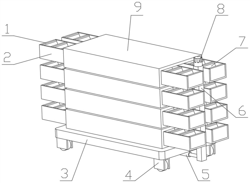
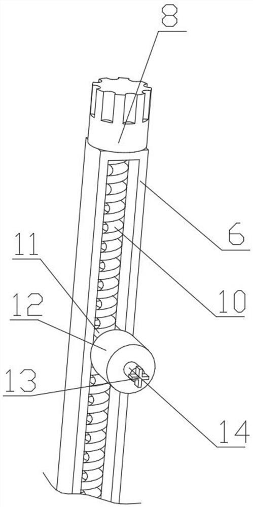
[0029] refer to Figure 1-5 , a transfer device for silicon wafer processing, comprising a base 3, the outer wall of the top of the base 3 is equipped with storage shells 9 equidistantly distributed, and the outer walls of both sides of the storage shell 9 are equipped with fixed blocks 16, and the two fixed blocks 16 are opposite to each other. One side of the outer wall is rotatably connected with the same two-way screw rod 15, and both sides of the circumference outer wall of the two-way screw rod 15 are connected with the first sliding block through screw thread rotation, and the outer walls at both ends of the first sliding block are equipped with a storage case 2. A rubber pad 21 is installed on the inner wall of the bottom of the housing 2, and the outer wall of the top of the rubber pad 21 is equipped with partitions 1 distributed equidistantly, and the top of the outer wall on the opposite side of the adjacent two partitions 1 is hinged with an extrusion plate 7, and t...

Embodiment 2

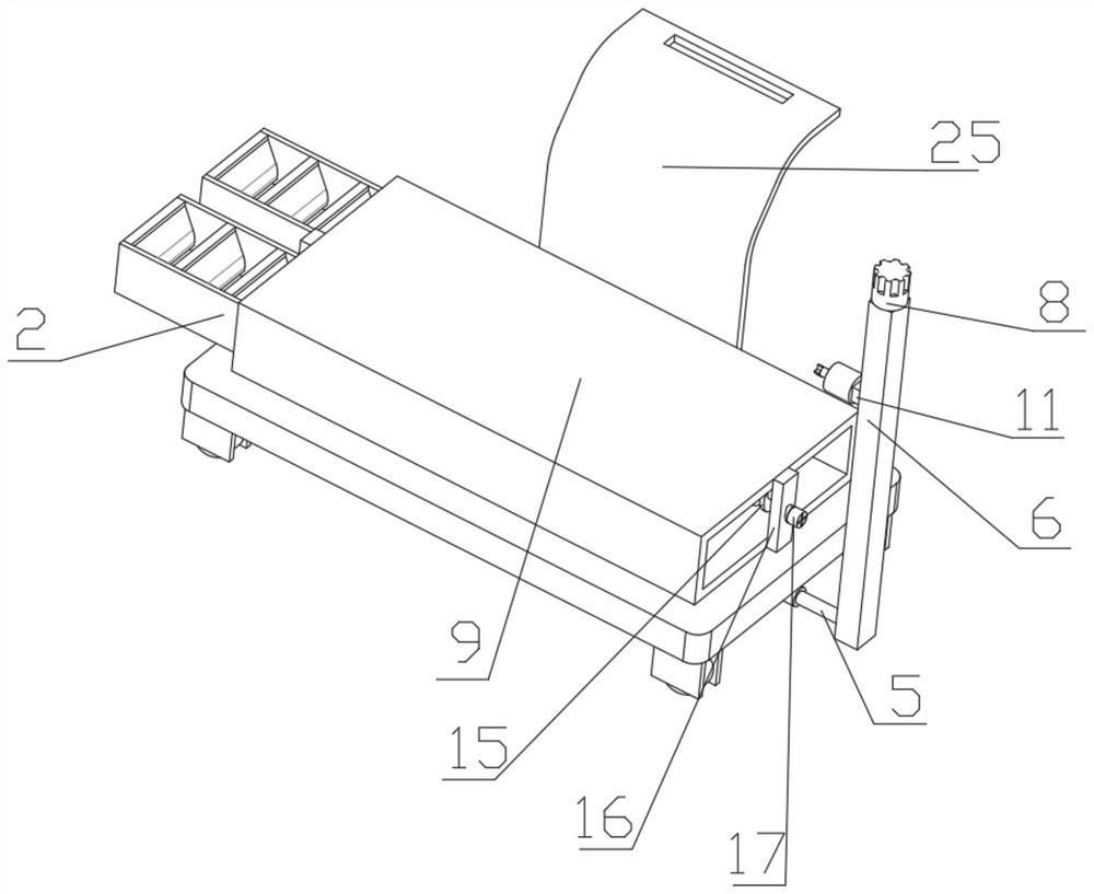
[0033] refer to Figure 1-6 , a transfer device for silicon wafer processing, which also includes a label holder 23 installed on the outer wall of one end of the storage housing 9, and equidistantly distributed stoppers 24 are installed on the inner wall of the bottom of the label holder 23.

[0034] Working principle: Compared with Embodiment 1, by setting the stopper 24 and the label rack 23, the stored silicon wafers can be recorded, which is convenient for staff to check and people to use.


PUM


Abstract

The invention discloses a transfer device for silicon wafer processing, which comprises a base, storage shells equidistantly distributed are installed on the outer wall of the top of the base, and fixed blocks are installed on the outer walls of both sides of the storage shell, and the two fixed blocks The outer wall on the opposite side is rotatably connected to the same two-way screw rod, and both sides of the outer wall of the two-way screw rod are connected to the first sliding block through screw thread rotation, and the outer walls at both ends of the first sliding block are equipped with storage housings for storage. A rubber pad is installed on the inner wall of the bottom of the housing, and the outer wall of the top of the rubber pad is equipped with partitions distributed equidistantly, and the top of the outer wall on the opposite side of two adjacent partitions is hinged with an extrusion plate. In the present invention, the storage case can be moved quickly by being provided with a two-way screw rod, a first sliding block, a fixed block and a partition plate, so that it can be stored conveniently. Squeezing it increases the fixation rate and prevents movement of the wafer during movement.

Description

technical field [0001] The invention relates to the technical field of silicon wafer processing, in particular to a transfer device for silicon wafer processing. Background technique [0002] On a silicon chip the size of a grain of rice, 160,000 transistors have been integrated, which is another milestone in the progress of science and technology. The silicon element with a content of 25.8% in the earth's crust provides an inexhaustible source for the production of monocrystalline silicon. Since silicon is one of the most abundant elements in the earth's crust, for products destined to enter the mass market, such as solar cells, the advantage of reserves is also one of the reasons why silicon has become the main material for photovoltaics. [0003] With the rapid development of the semiconductor industry, the production capacity of semiconductor silicon wafers is expanding day by day. In silicon wafer processing enterprises, in order to ensure the safety of silicon wafer p...

Claims


Application Information

Patent Timeline
Patent Type & Authority Patents(China)
IPC IPC(8): B62B3/00B62B3/04B62B5/00
CPCB62B3/008B62B3/04B62B5/00
Inventor 杨兆安
Owner 嘉兴市耐思威精密机械有限公司
Features
  • R&D
  • Intellectual Property
  • Life Sciences
  • Materials
  • Tech Scout
  • Unparalleled Data Quality
  • Higher Quality Content
  • 60% Fewer Hallucinations
Learn More